Pixel structure

A technology of pixel structure and pixel electrode, which is applied in the direction of static indicators, etc., can solve the problems of increased impedance and the inability of the proposed wiring to be used as a backup line for scanning wiring or data wiring, etc., to achieve the effect that the signal cannot be transmitted

Inactive Publication Date: 2005-01-12
AU OPTRONICS CORP
View PDF0 Cites 0 Cited by
  • Summary
  • Abstract
  • Description
  • Claims
  • Application Information

AI Technical Summary

Problems solved by technology

However, such a design has a disadvantage. If at least one of the two contact holes is not penetrated due to a defect in the manufacturing process, the intended wiring cannot be used as a backup line for the scan wiring or the data wiring after they are broken.
Therefore, as long as it is found that one of the two contact holes is not penetrated, the contact hole must be penetrated by laser repair, and the laser repair has the problem of increasing the impedance.

Method used


Image

  • Pixel structure
  • Pixel structure
  • Pixel structure

Examples


Embodiment Construction

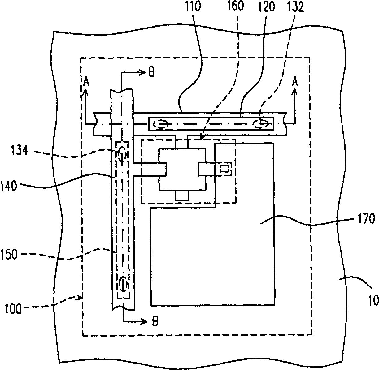
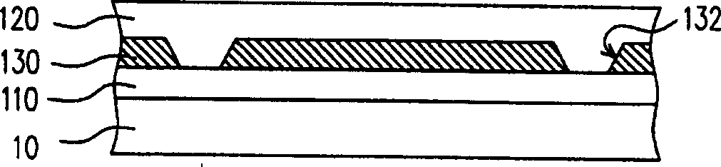
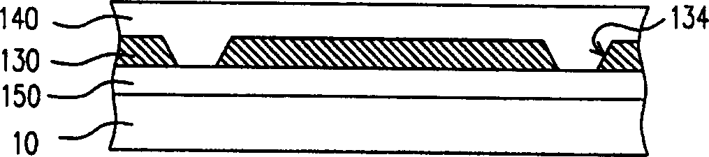
[0030] Figure 4 A top view showing a pixel structure with quasi-wiring according to a preferred embodiment of the present invention, Figure 5 is based on Figure 4 The side view seen on the section line C-C, while Figure 6 is based on Figure 4 Side view as seen on section line D-D. Please also refer to Figure 4 , Figure 5 as well as Figure 6, the pixel structure 200 of the present invention is constructed on a substrate 20, and the pixel structure 200 is mainly composed of a scanning wiring 210, a pseudo-scanning wiring 220, a dielectric layer 230, a data wiring 240, a pseudo- The data wiring 250 , an active element 260 and a pixel electrode 270 are formed.

[0031] The scanning wiring 210 and the data wiring 240 are arranged on the substrate 20 , and the intended scanning wiring 220 is arranged above the scanning wiring 210 , and the intended data wiring 250 is arranged under the data wiring 240 . The dielectric layer 230 is disposed between the scan wiring 210...


PUM

PropertyMeasurementUnit
Sizeaaaaaaaaaa

Abstract

The drawing structure is suitable configured on a base plate. For example, more than three contact holes are formed on dielectric layer between scanning data wires and scanning data quasi wires so as to make electrical connection between scanning data wires and scanning data quasi wires. When the said contact holes are not all passed through, signals are still can be transferred through scanning data quasi wires.

Description

technical field [0001] The present invention relates to a pixel structure (pixel), in particular to a pixel structure capable of avoiding contact holes not being penetrated due to process defects, that is, failure of intended wiring. Background technique [0002] In order to match the modern life style, the volume of video or image devices is becoming thinner and lighter. Although the traditional CLD still has its advantages, it needs to occupy a large volume and consumes a lot of power. Therefore, in combination with optoelectronic technology and semiconductor manufacturing technology, panel-type displays have been developed into common display products, such as liquid crystal displays (LCDs). [0003] The liquid crystal display is mainly composed of an active element array substrate, a color filter array substrate and a liquid crystal layer, wherein the active element array substrate is composed of a plurality of pixel units arranged in an array. The pixel unit is mainly...

Claims


Application Information

Patent Timeline
IPC IPC(8): G02F1/133
Inventor 来汉中
Owner AU OPTRONICS CORP
Why Eureka
Try Eureka