Wire bonding packaging body

A technology of wire bonding and packaging, which is applied in the direction of electric solid-state devices, semiconductor devices, semiconductor/solid-state device components, etc., can solve problems affecting the overall performance of multi-chip wire bonding package 10, and save production time and cost, improve overall performance, and avoid coupling effects

Active Publication Date: 2005-07-20
ALICORP
View PDF0 Cites 5 Cited by
  • Summary
  • Abstract
  • Description
  • Claims
  • Application Information

AI Technical Summary

Problems solved by technology

[0005] In addition, even if the first crystal grain 12 and the second crystal grain 14 have been redesigned before being arranged in the housing 16, the above-mentioned wire crossing situation will not occur, however, with the housing (for package) and the volume of the die is getting smaller and smaller, and the circuit in the die is becoming more and more complicated, the transmission is electrically connected to the pin 92 of the housing 16 and the die of the first die 12 Signals on the bonding wires 72 between the die bonding pads 82 are often transmitted between the pins 90 electrically connected to the housing 16 and the die bonding of the first die 12 due to the coupling effect caused by wire crowding. The effect of the signal on the bonding wire 70 between the pads 80 and indirectly affects the overall performance of the multi-die wire bonding package 10, especially when the signal transmitted on the bonding wire 72 is an analog signal.

Method used


Image

  • Wire bonding packaging body
  • Wire bonding packaging body
  • Wire bonding packaging body

Examples


Embodiment Construction

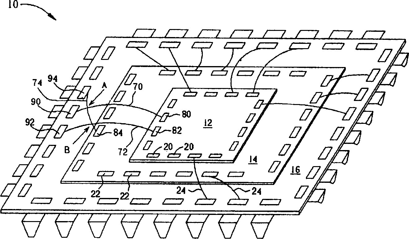
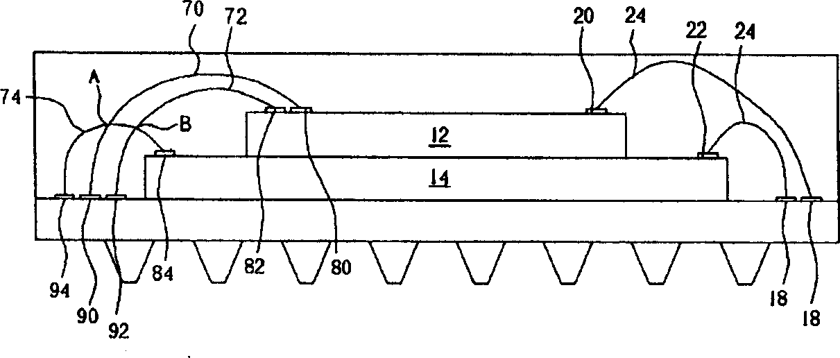
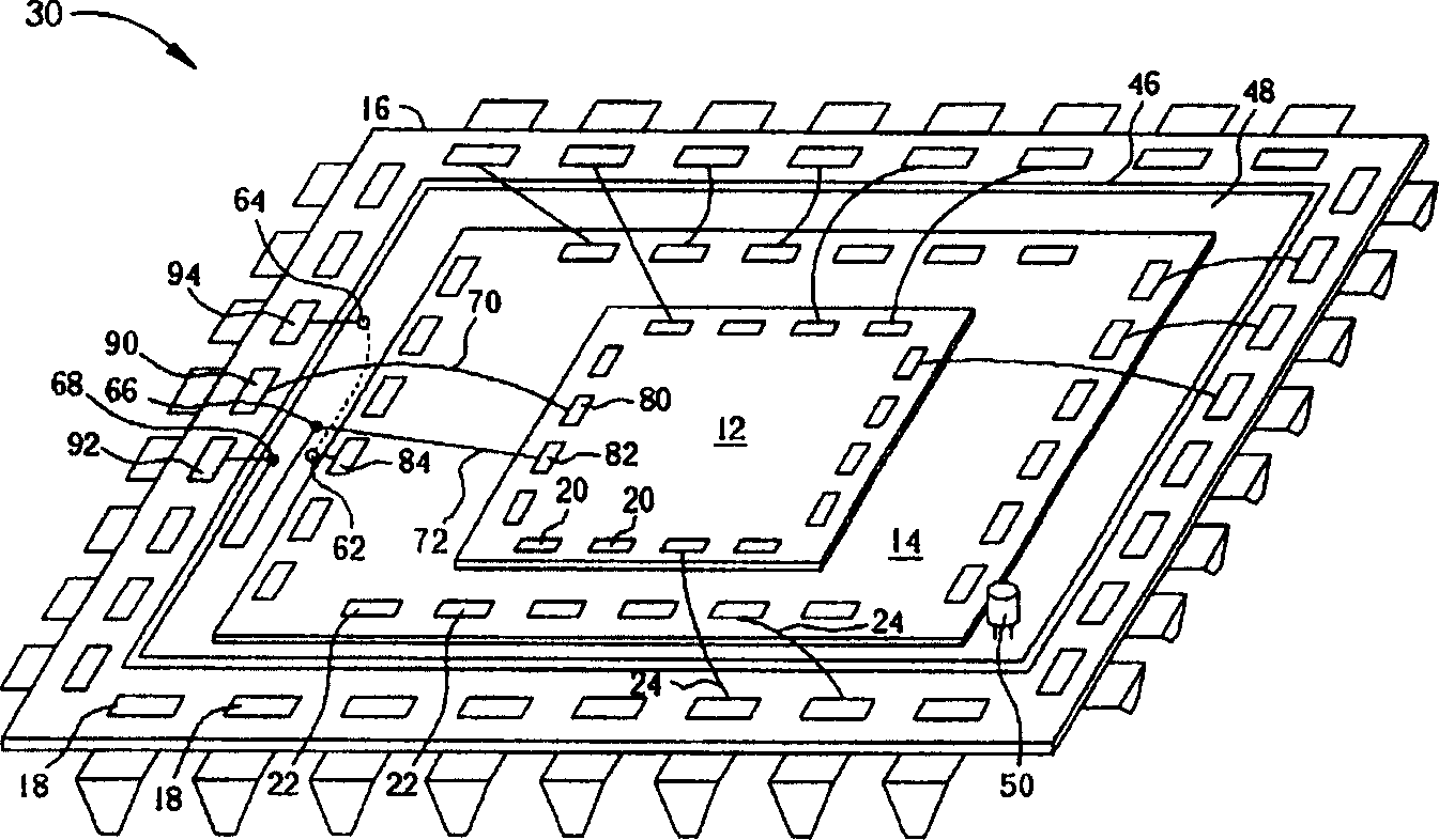
[0016] see image 3 and Figure 4 , image 3 It is a schematic diagram of a wire bonding package 30 in a preferred embodiment of the present invention, Figure 4 It is a side view of the wire bonding package 30 . In addition to the first die 12, the second die 14, the shell 16 and a plurality of pins for electrically connecting the die pads 20 and 22 on the first die 12 and the second die 14 to the shell 16 In addition to the bonding wires 24 on 18 , the wire bonding package 30 further includes a circuit board 48 disposed within the lead frame 46 of the housing 16 .

[0017] In a preferred embodiment of the present invention, the casing 16 is a quad flatpack (QFP), and the circuit board 48 is a double-layer circuit board. However, in the wire bonding package of the present invention, the housing 16 can also be a ball grid array (BGA) or a dual in-line package (DIP), The circuit board 48 can also be a multi-layer circuit board with a single layer or more than two layers. ...


PUM


Abstract

The invention provides a throwing jointing packaging body. It includes one shell body with many foot, one circuit board set in the shell body, no less than one crystal grain set on the circuit board, no less than welding cushion connected to the crystal grain, and joint lead wire on the circuit board. The joint leas wire can make the welding cushion on the crystal grain electronically connect to the food of the shell body.

Description

technical field [0001] The present invention relates to a wire bonding package, in particular to a wire bonding package in which dies can be electrically connected to pins on a housing via a circuit board. Background technique [0002] In the modern information society, microprocessor systems composed of integrated circuits have long been widely used in all aspects of life, such as personal computers, mobile communication equipment, and automatically controlled household appliances. The most important part is the die produced by the semiconductor manufacturing process. Die can be formed by a semiconductor manufacturing process: a wafer is cut into multiple regions, and various circuits are formed on individual regions to form the die. In addition to being directly electrically connected to a circuit board through the bare chip configuration method, the completed chip can also be packaged in a package in order to obtain the operating voltage or other data required for operat...

Claims


Application Information

Patent Timeline
Patent Type & Authority Applications(China)
IPC IPC(8): H01L23/02H01L23/12H01L23/48
CPCH01L2224/48091H01L2224/49171H01L2224/48227
Inventor 邱玉玲陈君明洪卫周
Owner ALICORP
Why Eureka
Try Eureka