Light-emitting-diode chip comprising sequence of gan-based epitaxial layers which emit radiation, and method for producing same

A technology of light-emitting diodes and epitaxial layers, applied in semiconductor devices, electrical components, circuits, etc., can solve the problems of increasing manufacturing costs, achieve effective cooling, reduce forward voltage, and improve wavelength stability

Inactive Publication Date: 2005-07-27
OSRAM OPTO SEMICON GMBH & CO OHG
View PDF1 Cites 0 Cited by
  • Summary
  • Abstract
  • Description
  • Claims
  • Application Information

AI Technical Summary

Problems solved by technology

[0007] However, said first proposal has the disadvantage that the radiation is largely absorbed by said contact layer
Additional processing steps are required in the second proposal, which significantly increases manufacturing costs

Method used


Image

  • Light-emitting-diode chip comprising sequence of gan-based epitaxial layers which emit radiation, and method for producing same
  • Light-emitting-diode chip comprising sequence of gan-based epitaxial layers which emit radiation, and method for producing same
  • Light-emitting-diode chip comprising sequence of gan-based epitaxial layers which emit radiation, and method for producing same

Examples


Embodiment Construction

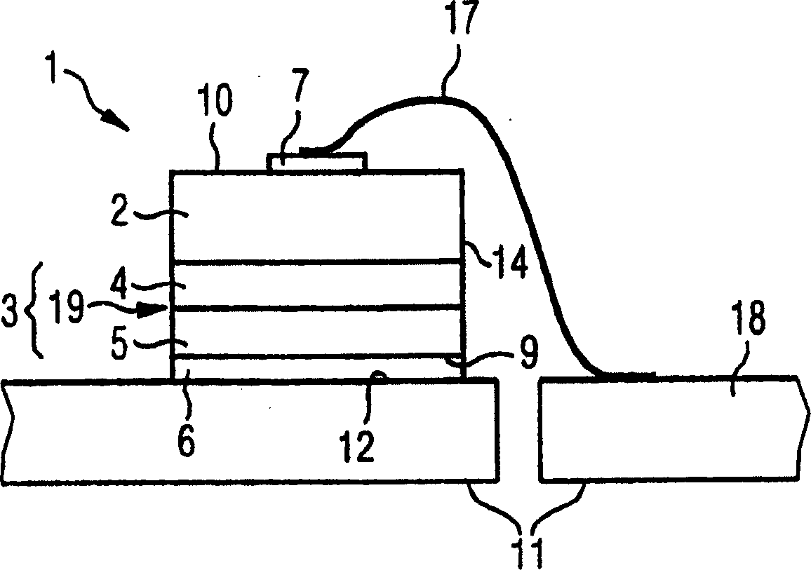
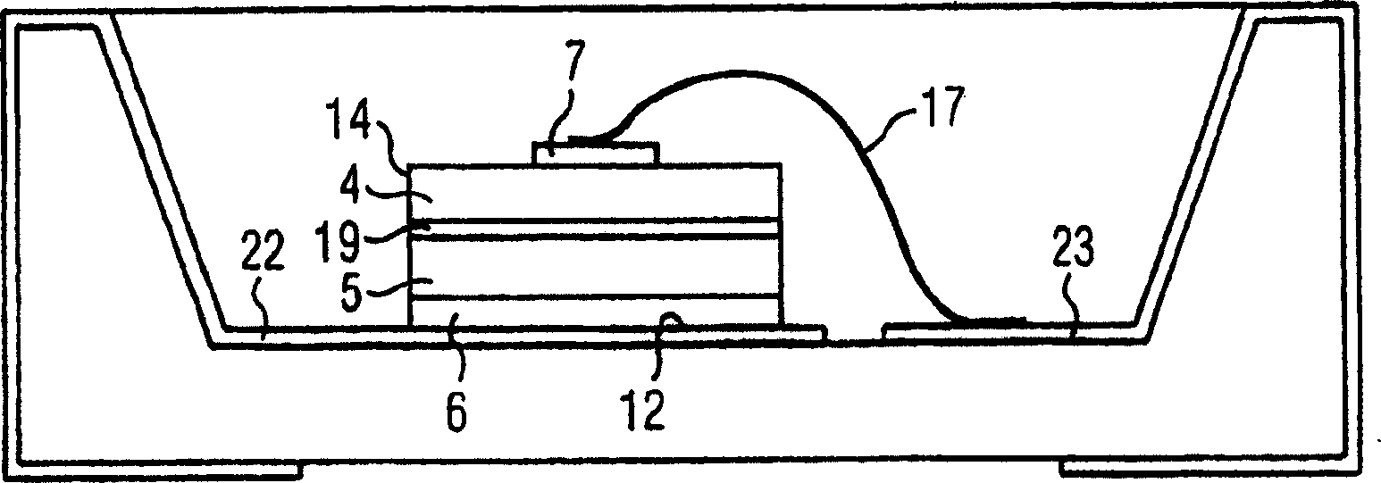
[0037] exist Figure 1a In the light-emitting diode chip 1 , a radiation epitaxial layer sequence 3 is applied on a SiC substrate 2 . The epitaxial layer sequence consists of an n-conductively doped GaN or AlGaN epitaxial layer 4 and a p-conductively doped GaN or AlGaN epitaxial layer 5 . Likewise, for example, a GaN-based epitaxial layer sequence 3 can be provided, which has a double heterostructure, a single quantum well (SQW) structure or a multiple quantum well (MQW) structure, which has one or more, eg, InGaN or Undoped layer 19 composed of InGaAlN.

[0038] Said SiC substrate 2 is electrically conductive and permeable to radiation emanating from the active region 19 of the epitaxial layer sequence 3 .

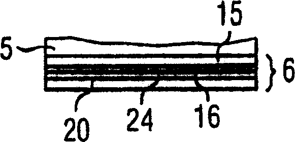
[0039] On its p-side 9 facing away from the SiC substrate 2 , a reflective and solderable Ag-based contact metallization 6 is applied over the entire surface of the epitaxial layer sequence 3 . The metal layer consists, for example, essentially of Ag, PtAg and / or PdAg ...


PUM


Abstract

A light-emitting diode chip ( 1 ) comprises a GaN-based, radiation-emitting epitaxial layer sequence ( 3 ), an active region ( 19 ), an n-doped layer ( 4 ) and a p-doped layer ( 5 ). The p-doped layer ( 5 ) is provided, on its main surface ( 9 ) facing away from the active region ( 19 ), with a reflective contact metallization ( 6 ) comprising a radioparent contact layer ( 15 ) and a reflective layer ( 16 ). Methods for fabricating LED chips of this type by thin-film technology are provided, as are LED components containing such LED chips.

Description

[0001] This application is a divisional application of the invention patent application with the application number of 01812915.3 and the application date of May 28, 2001, and the invention title is "Light Emitting Diode Chip with GaN-Based Radiation Epitaxial Layer Sequence and Its Manufacturing Method" . technical field [0002] The invention relates to a light-emitting diode chip with a GaN-based radiation epitaxial layer sequence, a method for producing the light-emitting diode chip, and a light-emitting diode device with such a light-emitting diode chip. Background technique [0003] “GaN-based” is understood below to mean in particular all ternary and quaternary GaN-based mixed crystals, such as AlN, InN, AlGaN, InGaN, InAlN and AlInGaN, as well as GaN itself. [0004] A fundamental problem in the manufacture of GaN-based light-emitting diode chips is that the highest electrical conductivity achievable with p-doped layers, especially p-doped GaN or AlGaN layers, is not...

Claims


Application Information

Patent Timeline
Patent Type & Authority Applications(China)
IPC IPC(8): H01L33/00H01L33/40
CPCH01L2924/01067H01L33/0079H01L2224/48091H01L2224/73265H01L2924/12041H01L33/405H01L2224/48227H01L2224/32225H01L24/73H01L33/0093H01L33/32H01L33/42H01L2924/00014H01L2924/00012
Inventor B·哈恩U·雅各布H·-J·卢高尔M·蒙布罗德-范格罗
Owner OSRAM OPTO SEMICON GMBH & CO OHG
Why Eureka
Try Eureka