Light-emitting-diode chip comprising sequence of GAN-based epitaxial layers which emit radiation, and method for producing same

一种发光二极管、外延层的技术,应用在电气元件、电固体器件、电路等方向,能够解决增加制造费用等问题,达到有效冷却、提高波长稳定性的效果

Inactive Publication Date: 2006-04-19
OSRAM OPTO SEMICON GMBH & CO OHG
View PDF0 Cites 0 Cited by
  • Summary
  • Abstract
  • Description
  • Claims
  • Application Information

AI Technical Summary

Problems solved by technology

[0006] However, said first proposal has the disadvantage that the radiation is largely absorbed by said contact layer
Additional processing steps are required in the second proposal, which significantly increases manufacturing costs

Method used


Image

  • Light-emitting-diode chip comprising sequence of GAN-based epitaxial layers which emit radiation, and method for producing same
  • Light-emitting-diode chip comprising sequence of GAN-based epitaxial layers which emit radiation, and method for producing same
  • Light-emitting-diode chip comprising sequence of GAN-based epitaxial layers which emit radiation, and method for producing same

Examples


Embodiment Construction

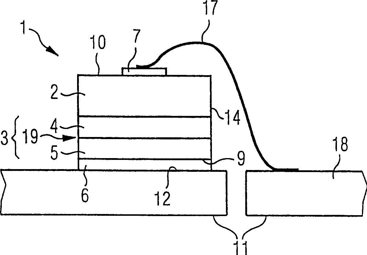
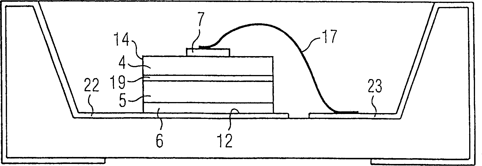
[0039] exist Figure 1a In the light-emitting diode chip 1 , a radiant epitaxial layer sequence 3 is applied on a SiC substrate 2 . The epitaxial layer sequence consists of an n-conductively doped GaN or AlGaN epitaxial layer 4 and a p-conductively doped GaN or AlGaN epitaxial layer 5 . Likewise, it is possible, for example, to set up a GaN-based epitaxial layer sequence 3 with a double heterostructure, a single quantum well (SQW) structure or a multiple quantum well (MQW) structure with one or more An undoped layer 19 composed of InGaAlN.

[0040] Said SiC substrate 2 is electrically conductive and transparent to radiation emanating from the active region 19 of the epitaxial layer sequence 3 .

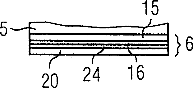
[0041] On its p-side 9 facing away from the SiC substrate 2 , a reflective but solderable Ag-based contact metallization 6 is applied over the entire surface of the epitaxial layer sequence 3 . The metal layer consists, for example, essentially of Ag, PtAg and / or PdAg alloys.

[0...


PUM


Abstract

A light-emitting diode chip ( 1 ) comprises a GaN-based, radiation-emitting epitaxial layer sequence ( 3 ), an active region ( 19 ), an n-doped layer ( 4 ) and a p-doped layer ( 5 ). The p-doped layer ( 5 ) is provided, on its main surface ( 9 ) facing away from the active region ( 19 ), with a reflective contact metallization ( 6 ) comprising a radioparent contact layer ( 15 ) and a reflective layer ( 16 ). Methods for fabricating LED chips of this type by thin-film technology are provided, as are LED components containing such LED chips.

Description

technical field [0001] The invention relates to a light-emitting diode chip with a GaN-based radiation epitaxial layer sequence, a method for producing the light-emitting diode chip, and a light-emitting diode component with such a light-emitting diode chip. Background technique [0002] “GaN-based” is understood below in particular to mean all ternary and quaternary GaN-based mixed crystals, such as AlN, InN, AlGaN, InGaN, InAlN and AlInGaN, as well as GaN itself. [0003] A fundamental problem in the fabrication of GaN-based light-emitting diode chips is that the highest conductivity achievable by p-doped layers, especially p-doped GaN or AlGaN layers, is insufficient to The current expansion takes place over the entire cross-section of the chip, wherein said metal layer is known from other material systems for light-emitting diode chips (for the highest possible radiation coupling-out, this metal layer only covers a part of the front side small portion). [0004] The gr...

Claims


Application Information

Patent Timeline
Patent Type & Authority Patents(China)
IPC IPC(8): H01L33/00H01L33/40
CPCH01L33/405H01L2924/12041H01L2224/32225H01L33/0079H01L2224/48091H01L2224/48227H01L2924/01067H01L2224/73265H01L24/73H01L33/0093H01L33/32H01L33/42H01L2924/00014H01L2924/00012
Inventor B·哈恩U·雅各布H·-J·卢高尔M·蒙布罗德-范格罗
Owner OSRAM OPTO SEMICON GMBH & CO OHG
Why Eureka
Try Eureka