Nitride semiconductor light emitting device and method for fabricating the same

a light emitting device and semiconductor technology, applied in semiconductor/solid-state device manufacturing, semiconductor devices, electrical equipment, etc., can solve the problems of difficult to obtain a good nitride semiconductor crystal on the substrate made of si, difficult to further increase the diameter, and further cost reduction limitations, so as to improve the light extraction efficiency of a nitride semiconductor light emitting devi

Inactive Publication Date: 2008-07-31
PANASONIC CORP
View PDF20 Cites 86 Cited by
  • Summary
  • Abstract
  • Description
  • Claims
  • Application Information

AI Technical Summary

Benefits of technology

[0009]In view of the conventional problems, an object of the present invention is to reduce the absorption of emitted light by a substrate for crystal growth to improve light extraction efficiency of a nitride semiconductor light emitting device.

Problems solved by technology

It is difficult to further increase the diameter of the substrate whose principal surface is a C plane (plane direction is a (0001) plane) used for the crystal growth, and it is thought that a further cost reduction is limited.
Since silicon and the nitride-based semiconductor are greatly different in lattice constant and in thermal expansion coefficient, it has been difficult to obtain a good nitride semiconductor crystal on the substrate made of Si.
However, if a Si substrate is used as a substrate for growth of the conventional nitride semiconductor and a light emitting diode is formed on the Si substrate, a problem arises that the light power of the light emitting diode is reduced.

Method used


Image

  • Nitride semiconductor light emitting device and method for fabricating the same
  • Nitride semiconductor light emitting device and method for fabricating the same
  • Nitride semiconductor light emitting device and method for fabricating the same

Examples


embodiment 1

Variation 2 of Embodiment 1

[0108]Variation 2 of Embodiment 1 of the present invention will be described below with reference to the drawings.

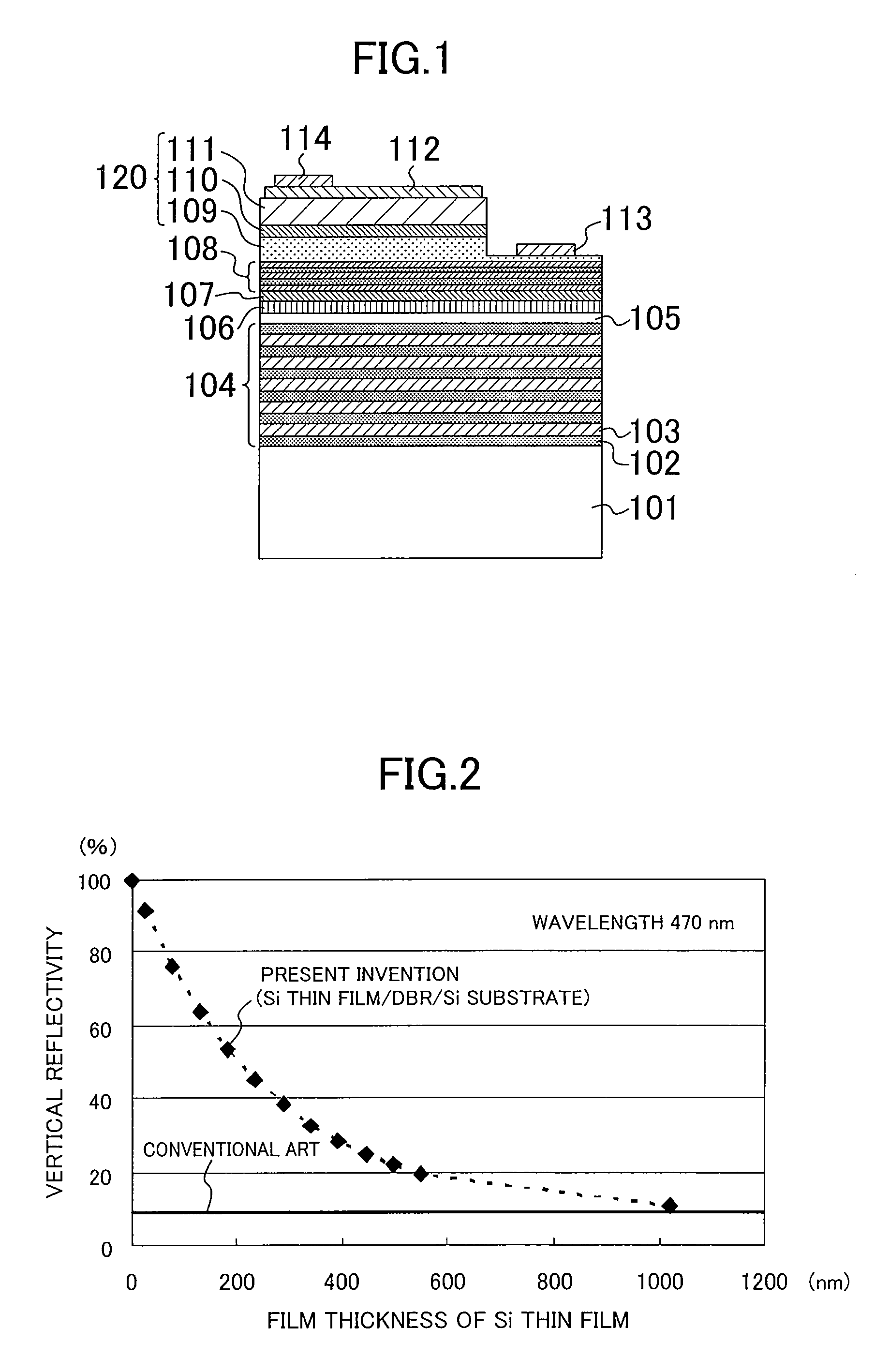
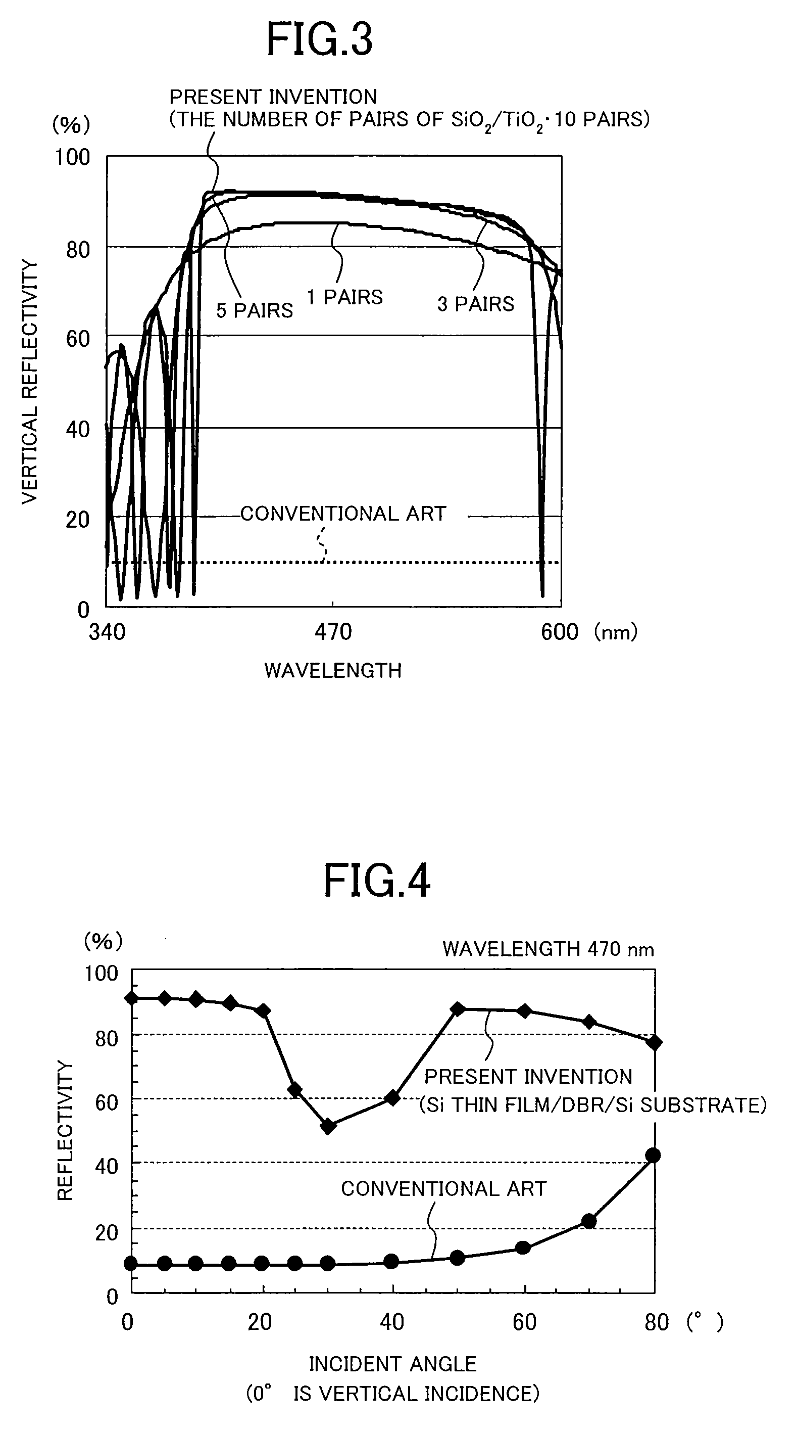
[0109]FIG. 9 shows a cross sectional structure of a light emitting diode of Variation 2 of Embodiment 1 of the present invention. In FIG. 9, the same components as those of FIG. 1 are indicated by the same numerals and descriptions thereof are omitted.

[0110]As shown in FIG. 9, the light emitting diode of Variation 2 includes a conductive member 122 formed in a through-hole 101a, wherein the conductive member 122 electrically connects the n-side electrode 113 with the substrate 101 and is made of gold (Au). The through-hole 101a is formed through the n-type cladding layer 109, the cycle structure 108, the interlayer 107, the initial layer 106, the semiconductor thin film 105, and the multilayer DBR mirror 104 to an upper portion of the substrate 101. The through-hole 101a can be formed by performing dry etching using an etching gas whose main co...

embodiment 2

Variation 2 of Embodiment 2

[0147]Variation 2 of Embodiment 2 of the present invention will be described below with reference to the drawings.

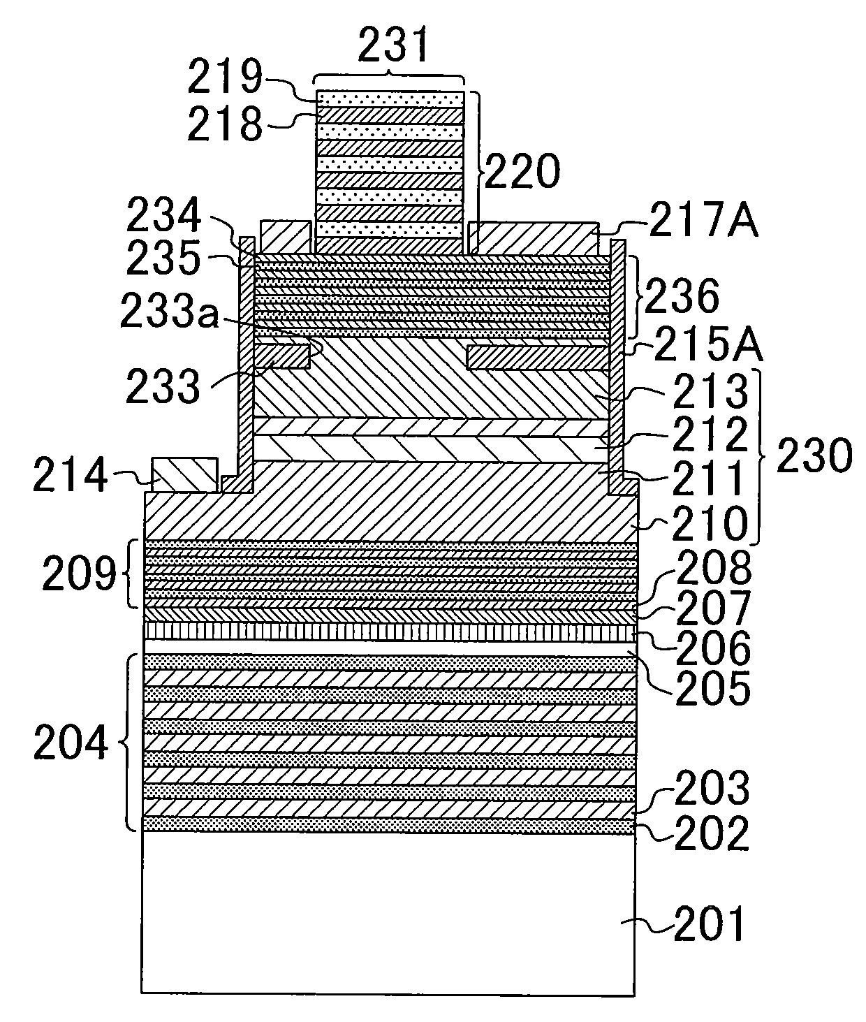
[0148]FIG. 15 shows a cross sectional structure of a surface emitting laser device of Variation 2 of Embodiment 2 of the present invention. In FIG. 15, the same components as those of FIG. 10B are indicated by the same numerals and descriptions thereof are omitted.

[0149]As shown in FIG. 15, the surface emitting laser device of Variation 2 is selectively provided with a current confinement layer 233 instead of the current confinement layer 215. The current confinement layer 215 is made of SiO2 selectively covering the side surface and part of the upper surface of the p-type cladding layer 213 of surface emitting laser device of Embodiment 2. The current confinement layer 233 is made of SiO2 having an opening 233a in an upper portion of the p-type cladding layer 213 and having a thickness of, for example, 100 nm.

[0150]Moreover, in Variation 2, a ...


PUM


Abstract

A nitride semiconductor light emitting device includes: a dielectric layered film over a substrate, the dielectric layered film being formed by stacking a plurality of dielectric films having different compositions; a semiconductor thin film formed of a single crystal over the dielectric layered film; and a pn junction diode structure over the semiconductor thin film, the pn junction diode structure being formed of a nitride semiconductor.

Description

CROSS-REFERENCE TO RELATED APPLICATION(S)[0001]This application claims priority under 35 U.S.C. §119(a) on Japanese Patent Application No. 2007-18484 filed on Jan. 29, 2006, the entire contents of claims, specification, and drawings of which are hereby incorporated by reference.BACKGROUND OF THE INVENTION[0002]1. Field of the Invention[0003]The present invention relates to a nitride semiconductor light emitting device applicable to a light emitting diode for emitting visible light or white light for example and to a method for fabricating the same.[0004]2. Description of the Prior Art[0005]A so-called nitride-based compound semiconductor (expressed by a general formula, InxAlyGa1-x-yN (where 0≦x≦1, 0≦y≦1, and x+y≦1)) typified by gallium nitride (GaN) realizes a light emitting device having a wide wavelength range including visible light such as blue light and ultraviolet light. A wide application of a light emitting diode including a nitride semiconductor is considered and examples ...

Claims


Application Information

Patent Timeline
Patent Type & Authority Applications(United States)
IPC IPC(8): H01L33/00H01L33/10H01L33/06H01L33/20H01L33/32H01L33/42H01L33/44
CPCH01L33/007H01L33/0079H01L33/465H01L33/145H01L33/32H01L33/105H01L33/0093
Inventor TAKASE, YUJIUEDA, TETSUZOTANAKA, TSUYOSHIUEDA, DAISUKE
Owner PANASONIC CORP
Why Eureka
Try Eureka