
Optical semiconductor device and optical semiconductor integrated circuit

A semiconductor and optical waveguide technology, applied in the field of optical semiconductor components and optical semiconductor integrated circuits, can solve the problems of the limitation of the degree of freedom of the waveguide, the inability to use cleavage surfaces, and the difficulty in manufacturing, so as to improve the degree of freedom, suppress the deterioration of reliability, Effect of suppressing waveguide loss

Inactive Publication Date: 2005-11-23
NIPPON TELEGRAPH & TELEPHONE CORP
View PDF1 Cites 16 Cited by
  • Summary
  • Abstract
  • Description
  • Claims
  • Application Information

AI Technical Summary

Problems solved by technology

[0024] However, when a semiconductor optical waveguide is coupled to an optical waveguide made of a material having a different refractive index from the semiconductor optical waveguide, the degree of freedom in waveguide design is limited due to reflection at the bonding interface corresponding to the difference in refractive index.
[0025] where by using the Brewster angle θ B , the reflection between waveguides with different refractive indices can be reduced, but using the Brewster angle θ B If the light is refracted at the boundary surface between the waveguides, there is a problem that the waveguide direction becomes not a straight line.
[0026] In addition, Brewster's angle θ is used to reduce reflection between waveguides with different refractive indices. B If this is the case, it becomes difficult to fabricate a buried semiconductor waveguide along a specific crystal direction, and there is a problem that a buried semiconductor waveguide cannot be fabricated with high reliability.
[0027] Furthermore, if Brewster's angle θ is used to reduce reflection between waveguides with different refractive indices, B If this is the case, it is difficult to arrange the semiconductor waveguide perpendicular to the cleavage plane, and there is a problem that the cleavage plane cannot be used as a reflection surface of a semiconductor laser or the like.

Method used


Image

  • Optical semiconductor device and optical semiconductor integrated circuit
  • Optical semiconductor device and optical semiconductor integrated circuit
  • Optical semiconductor device and optical semiconductor integrated circuit

Examples


Embodiment Construction

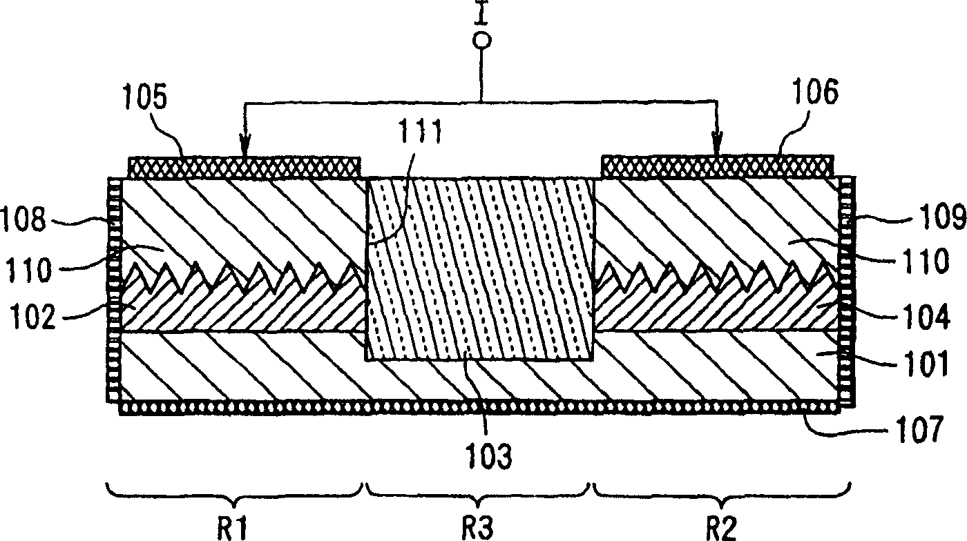
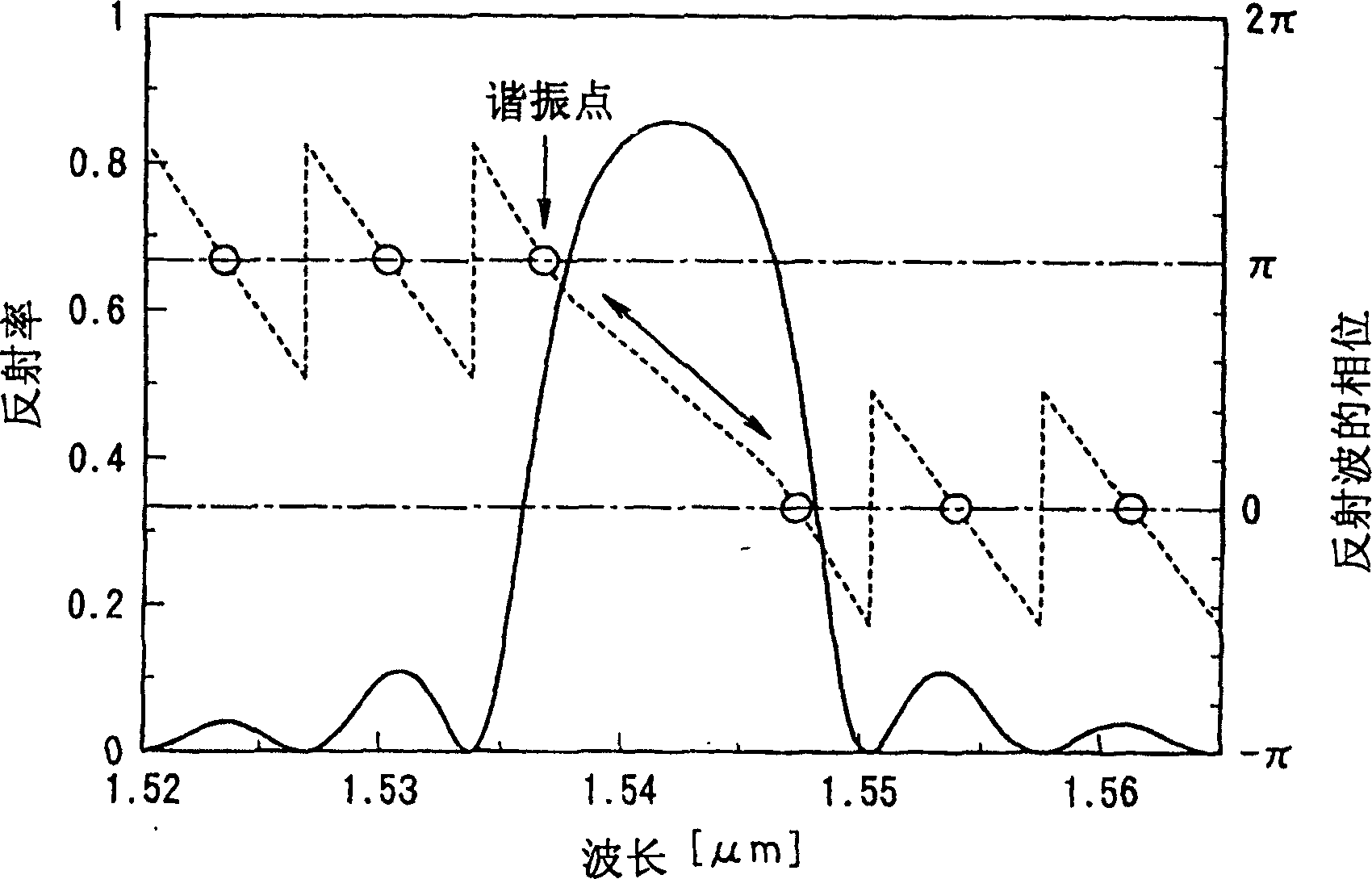
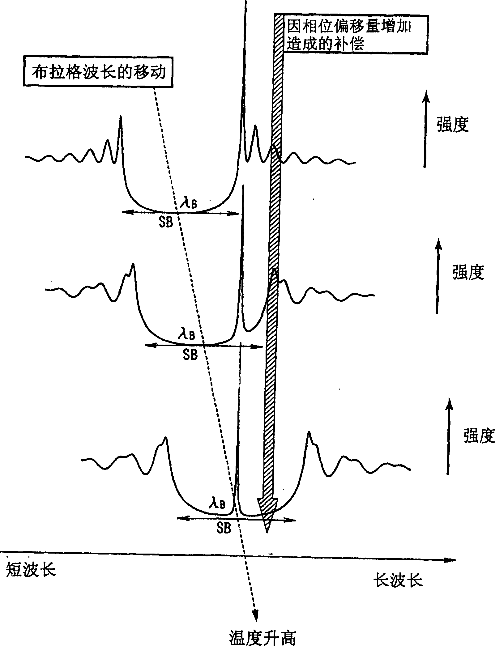
[0090] Several embodiments of the present invention will be described below with reference to the drawings. First, as a first embodiment, some examples of application examples to semiconductor lasers will be shown and described. In this embodiment mode, by combining a semiconductor laser with a material having a different temperature dependence of the refractive index, it is possible to control the temperature dependence of the vibration wavelength of the semiconductor laser.

[0091] As a second embodiment, some examples of application to integrated optical waveguides will be shown and described. In this embodiment, when integrating a semiconductor optical waveguide with an optical waveguide having a different refractive index and a temperature dependence of the refractive index, reflection at the interface between these optical waveguides can be reduced. In addition, by integrating a semiconductor optical waveguide with an optical waveguide having a different refractive ind...


PUM

PropertyMeasurementUnit
Coupling coefficientaaaaaaaaaa

Abstract

An optical semiconductor device and optical semiconductor integrated circuit are provided by combining, on a semiconductor substrate, materials having different refractive indices and different temperature dependence of the refractive indices. In particular, it becomes possible to control the temperature dependence of the oscillation wavelength with a propagating region having a material and / or structure whose temperature dependence of the refractive index is different from that of a gain region of the semiconductor laser. In addition, they can be configured to have a plurality of interfaces formed along the waveguide direction of the optical waveguide so that the light reflected off the first interface is weakened by the light reflected from the remaining interfaces. Also, they can be configured with the interfaces inclined to the propagating direction so that the waveguide loss due to the reflection and refraction between the optical waveguides whose refractive indices differ from each other can be reduced.

Description

technical field [0001] The present invention relates to optical semiconductor elements such as semiconductor lasers, optical waveguides, and other optical devices, and optical semiconductor integrated circuits, and more particularly to optical semiconductor elements in which materials having different refractive indices and temperature dependencies of refractive indices are combined on a semiconductor substrate and optical semiconductor integrated circuits. Background technique [0002] The vibration wavelength of semiconductor lasers changes with ambient temperature and element temperature. For example, as published by K.Sakai, "1.5μm range InGaAsP / InP distributed feedback lasers," IEEEJ.Quantum Electron., vol.QW-18, pp.1272-1278, Aug.1982, the distributed feedback type (DFB) laser The dependence of the vibration wavelength on temperature is about 0.1nm / K. This is due to the temperature dependence of the refractive index (n) of the semiconductor, so the Bragg wavelength (...

Claims


Application Information

Patent Timeline
IPC IPC(8): H01S5/12
Inventor 布谷伸浩柴田泰夫藤原直树菊池顺裕东盛裕一
Owner NIPPON TELEGRAPH & TELEPHONE CORP
Features
  • Generate Ideas
  • Intellectual Property
  • Life Sciences
  • Materials
  • Tech Scout
  • Unparalleled Data Quality
  • Higher Quality Content
  • 60% Fewer Hallucinations
Learn More