Nonvolatile semiconductor memory device and method of manufacturing the same

A non-volatile, storage device technology, used in semiconductor/solid-state device manufacturing, semiconductor devices, electrical solid-state devices, etc. Failure, effect of memory cell shrinkage

Inactive Publication Date: 2006-01-18
NEC ELECTRONICS CORP
View PDF1 Cites 7 Cited by
  • Summary
  • Abstract
  • Description
  • Claims
  • Application Information

AI Technical Summary

Problems solved by technology

Furthermore, as the trench 120 becomes deeper, it becomes more difficult to bury the oxide film in the trench 120, which causes formation of voids and thus causes failure of the memory device.

Method used


Image

  • Nonvolatile semiconductor memory device and method of manufacturing the same
  • Nonvolatile semiconductor memory device and method of manufacturing the same
  • Nonvolatile semiconductor memory device and method of manufacturing the same

Examples


Embodiment Construction

[0038] The invention will now be described herein with reference to illustrative embodiments. Those skilled in the art will recognize that many alternative embodiments can be accomplished using the teachings of the present invention and that the invention is not limited to the embodiments described for explanatory purposes.

[0039] (structure)

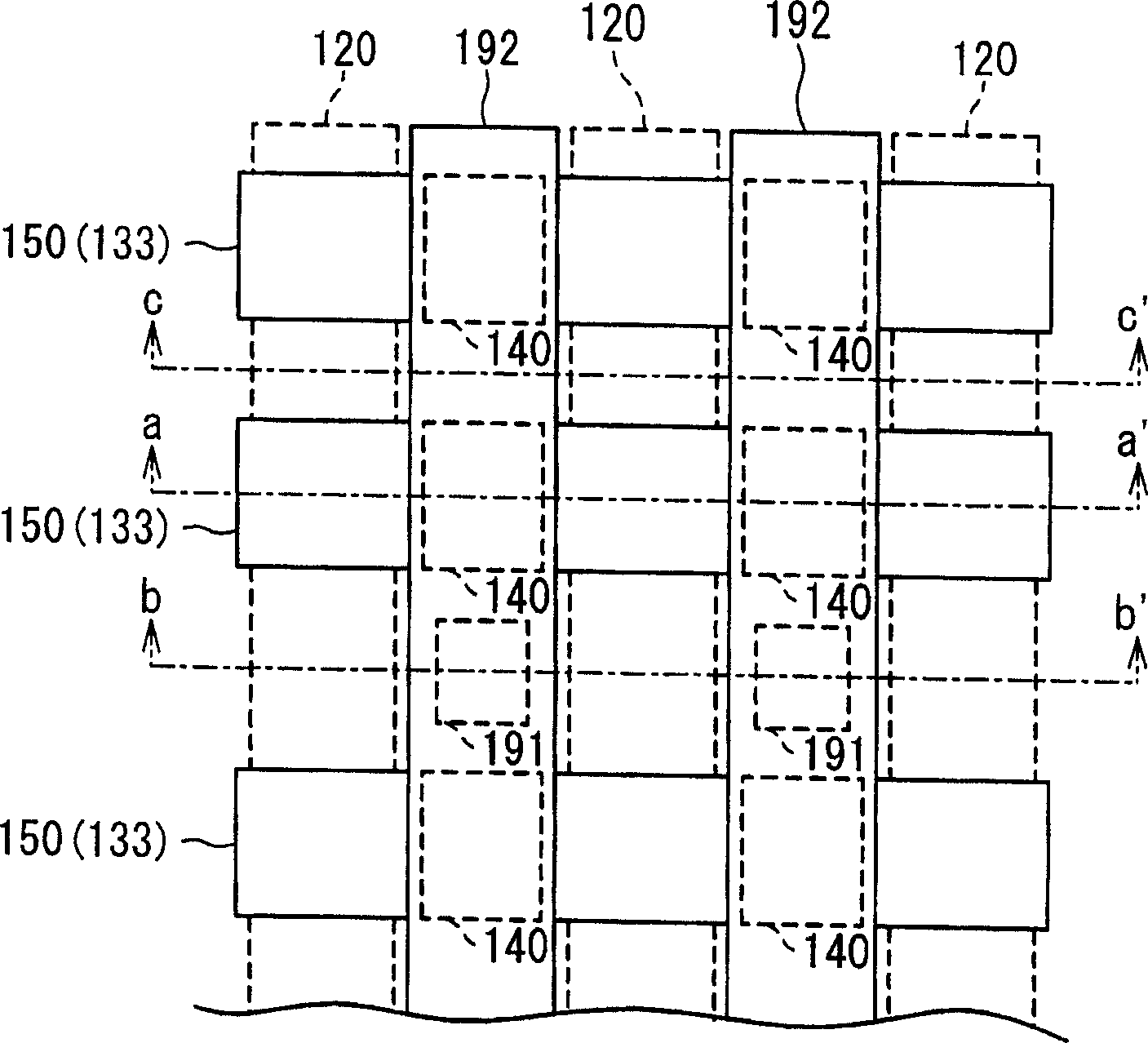
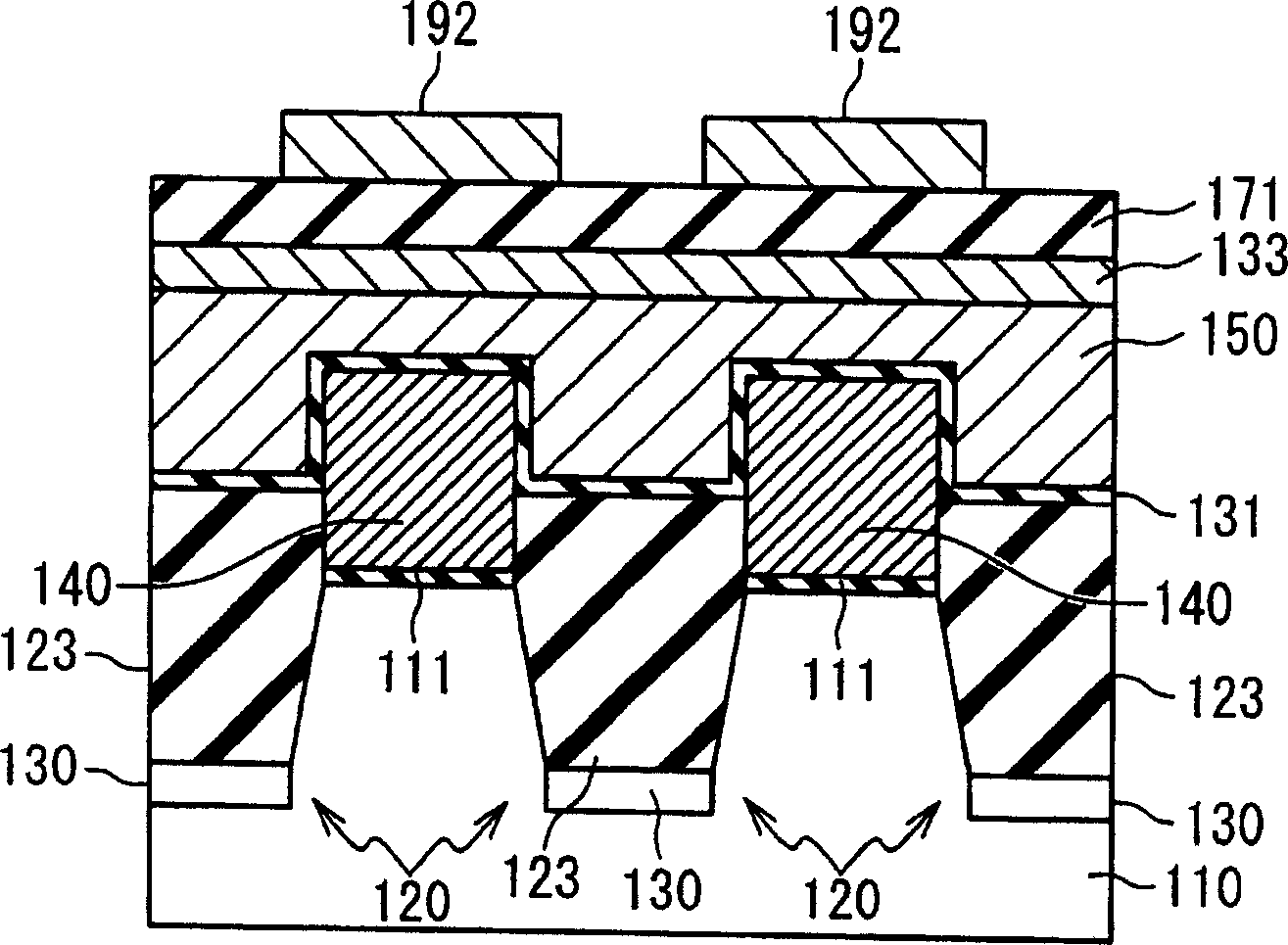
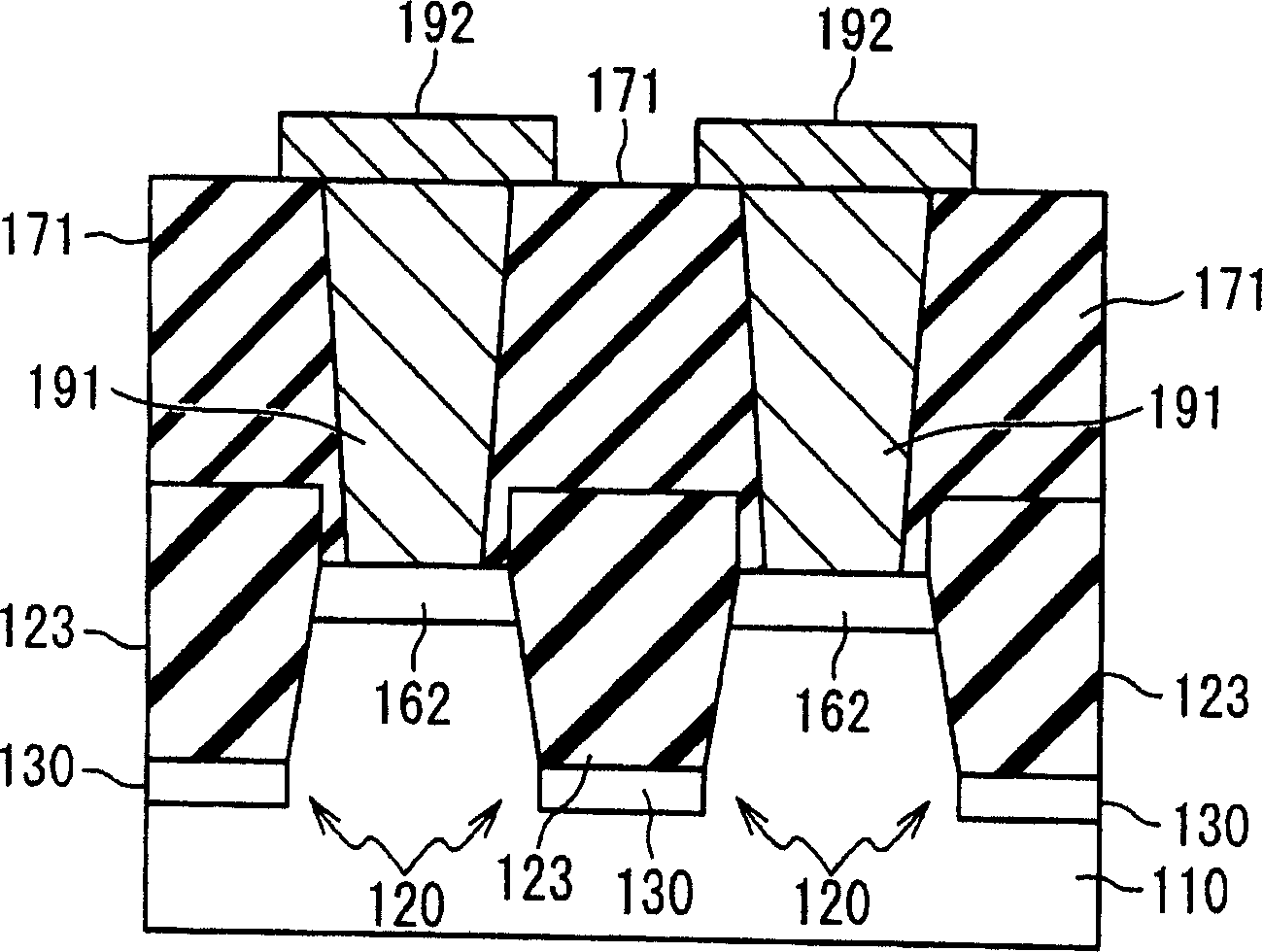
[0040] 3 is a plan view schematically showing the structure of a nonvolatile semiconductor memory device according to an embodiment of the present invention. Figures 4A to 4F They are cross-sectional views along the dotted lines A-A', B-B', C-C', D-D', E-E' and F-F' in Fig. 3, respectively.

[0041] In the nonvolatile semiconductor memory device 1, as shown in FIG. gate 50; metal film 33). The Z direction (third direction) is defined as the normal direction of the substrate. These X directions, Y directions and Z directions are orthogonal to each other. In FIG. 3, bit lines and word lines intersect at a plurality of intersection...


PUM


Abstract

A nonvolatile semiconductor memory device has a substrate, a floating gate, a buried gate, a control gate, and source / drain regions. The substrate has a trench formed in a first direction. The floating gate is formed on a surface of the substrate outside the trench through a first gate insulating film. The buried gate is formed on a surface of the trench through a second gate insulating film. The control gate is formed to cover the floating gate through a third gate insulating film. The source / drain regions are formed in the substrate below the floating gate.

Description

technical field [0001] The invention relates to a nonvolatile semiconductor storage device and a manufacturing method thereof. Background technique [0002] FIG. 1 is a plan view schematically showing the structure of a nonvolatile semiconductor memory device according to the related art. 2A to 2C are cross-sectional views of the nonvolatile semiconductor memory device along lines a-a', b-b' and c-c' in FIG. 1, respectively. [0003] As shown in FIGS. 1 and 2A to 2C, a nonvolatile semiconductor memory device 100 includes a substrate 110 having a trench 120, a floating gate 140 formed on the substrate 110 through a tunnel oxide film 111, An oxide-oxide (ONO) film 131 is formed to cover the control gate 150 , the source region 161 and the drain region 162 of the floating gate 140 . An oxide film 123 is buried in the trench 120, which is used for device isolation. Also, an impurity layer 130 is formed at the bottom of the trench 120 . Connected to control gate 150 is word l...

Claims


Application Information

Patent Timeline
Patent Type & Authority Applications(China)
IPC IPC(8): H01L27/105H01L29/788H01L21/8239H01L21/336
CPCH01L27/11521H01L29/42328H01L29/42336H01L27/115H10B69/00H10B41/30
Inventor 原英树
Owner NEC ELECTRONICS CORP
Why Eureka
Try Eureka