Wafer connector

A technology of connectors and wafers, which is applied in the direction of connection, parts of connection devices, incandescent lamps, etc., and can solve the problem of not scraping off the oxide layer

Inactive Publication Date: 2006-10-04
TOP YANG TECH ENTERPRISE CO LTD
View PDF0 Cites 0 Cited by
  • Summary
  • Abstract
  • Description
  • Claims
  • Application Information

AI Technical Summary

Problems solved by technology

[0005] The known structure has the following disadvantages: that is, when the terminal 12 is pressed down by the chip 90, it only simply bounces up and down, and the contact point of its contact portion 13 and the contact point 91 of the chip is almost at the same position, and the change is very small, so There is no friction between the two, and there is no effect of scraping off the oxide layer

Method used


Image

  • Wafer connector
  • Wafer connector
  • Wafer connector

Examples


Embodiment Construction

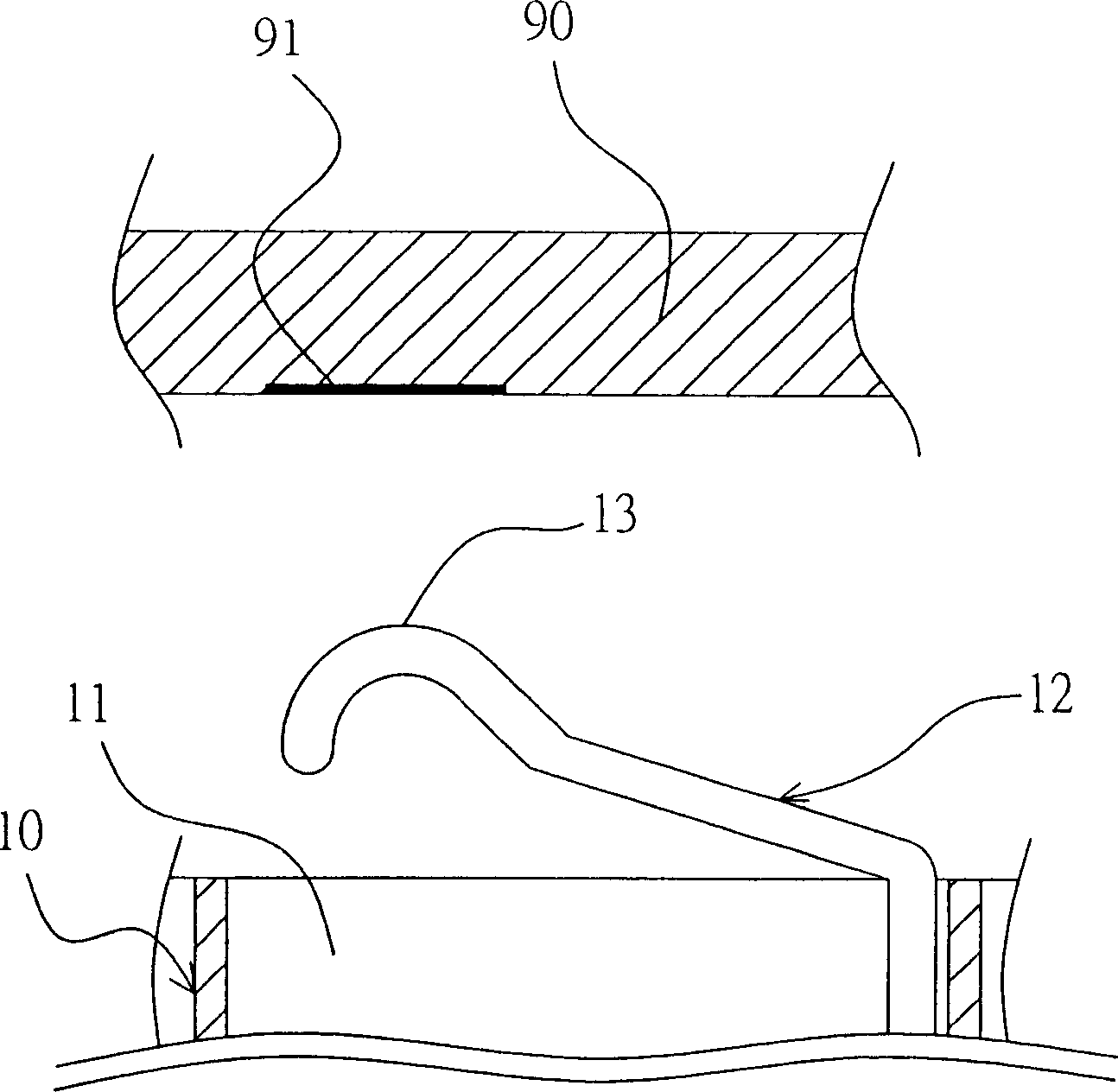
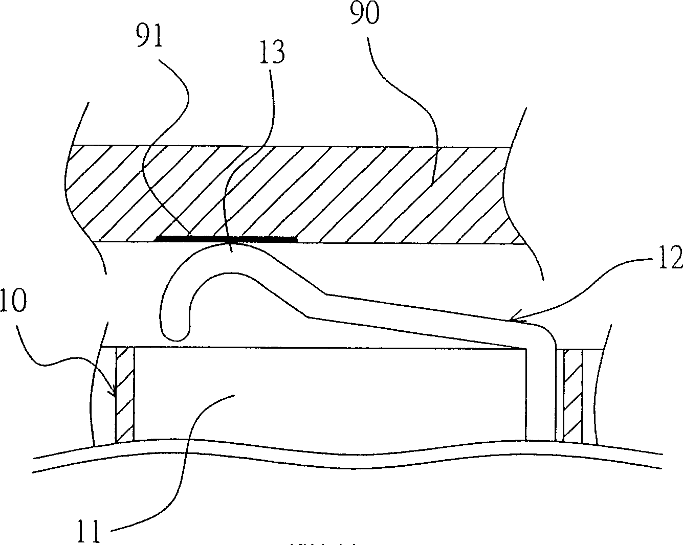
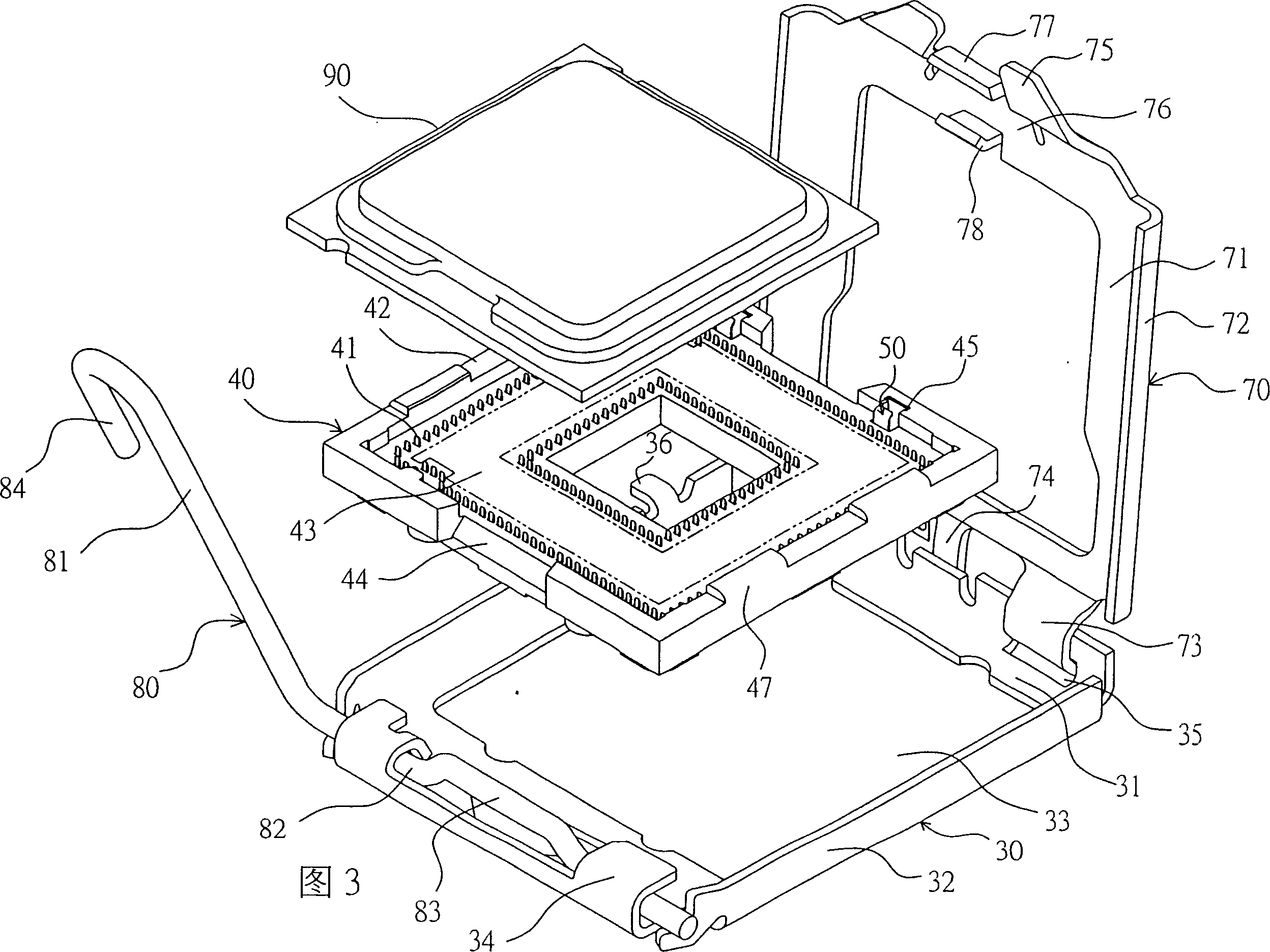
[0032] Please refer to Figure 3, Figure 4, Figure 5 and Figure 8 , the electrical connector of this embodiment includes: a base, an elastic device 50, several terminals 60, an upper cover 70, and a rocker 80, wherein:

[0033] The base includes a metal outer seat 30 and a plastic inner seat 40; the outer seat 30 is provided with a bottom surface 31 and two side walls 32, a hollow area 33 is formed in the center of the bottom surface 31, and a third A pivotal joint 34, and the rear end is provided with the second pivotal joint 35 that is hole-shaped, and the other side is provided with a clamping piece 36; Several terminal grooves 41 are arranged, and the periphery of its upper end is provided with upward flange 42 and surrounds a placement area 43 for placing wafer 90, and the front end flange of this placement area is provided with a gap 44, and the rear end is provided with two grooves 45, The upper ends of the flanges on both sides are provided with protruding bumps 47 . ...


PUM


Abstract

The invention provides a crystal chip connector which is used to electric connect a crystal chip. It comprises a base with a plurality of terminal grooves and a crystal chip position area, wherein the elastic device is positioned on the rear end of the base; a plurality of terminals are positioned in the plurality of terminal grooves; there are a touching part, an upper cover whose rear end is connected with the base and the front end has a projection, a first raising jack and a second raising jack; when the upper cover covers the base, it can press the crystal chip and the second raising jack can be on the front end of the crystal chip; the bell crank has vertical first crank and second crank, when the first crank bells to the rear end of the base, the projection crank can press the projection of the upper cover and pull the first raising jack of the upper cover so that the upper cover shifts to the rear end and pulls the second raising jack to let the crystal chip to move to the rear part.

Description

technical field [0001] The invention relates to an electrical connector, in particular to a chip connector. Background technique [0002] The bottom surface of a chip (such as a CPU) is formed with several contacts arranged at intervals, and the electrical connector connected to this type of chip uses a pressure to fix the chip on the base, so that the contacts of the chip are arranged in the terminal groove of the base. The terminals are elastically contacted to ensure electrical connection. [0003] see figure 1 , is an electrical connector for connecting chips, which is provided with: a base body 10, on which several terminal grooves 11 are arranged; and several terminals 12, which are arranged on the terminal grooves 11 of the base body, and are provided with a The contact part 13 can bounce up and down. [0004] When the chip 90 is placed on the base body 10, each contact 91 of the chip 90 is in contact with the contact portion 13 of each terminal 12; please refer to...

Claims


Application Information

Patent Timeline
Patent Type & Authority Applications(China)
IPC IPC(8): H01R33/76H01R13/629H01R13/631
Inventor 蔡周旋
Owner TOP YANG TECH ENTERPRISE CO LTD
Why Eureka
Try Eureka