

Open drain driver, and a switch comprising the open drain driver
一种开关电路、驱动器的技术,应用在电路、电子开关、电气元件等方向,能够解决上升、第二MOSFET失效等问题
- Summary
- Abstract
- Description
- Claims
- Application Information
AI Technical Summary
Problems solved by technology
Method used
Image

Examples
Embodiment Construction
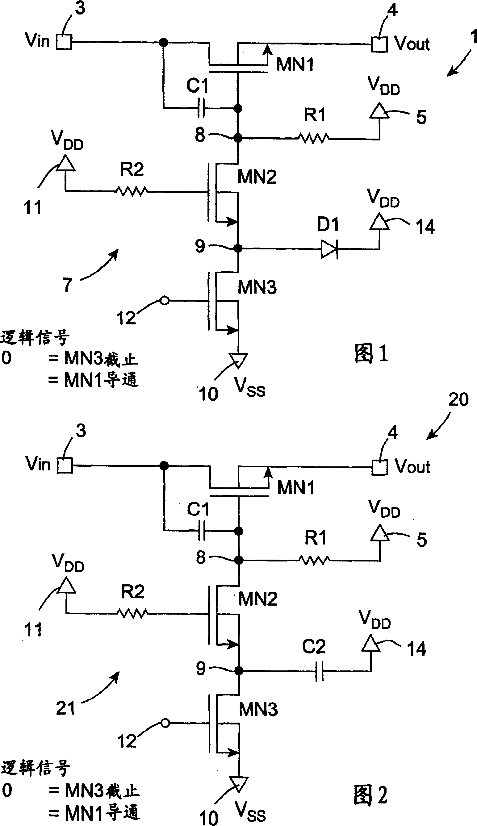
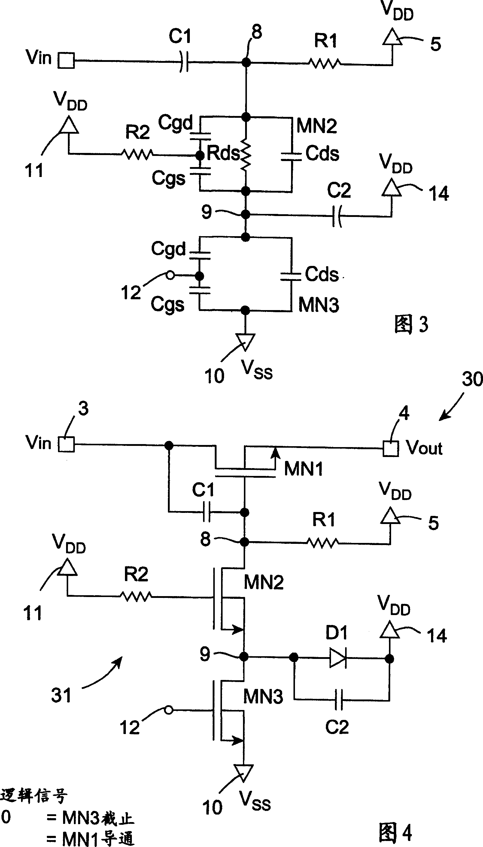
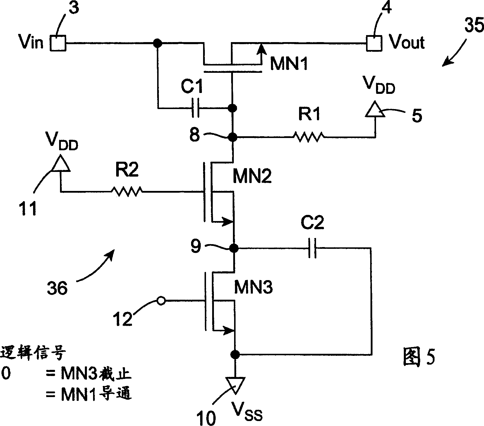
[0091] Referring to the drawings and initially to FIG. 1 , there is shown a switching circuit according to the invention, generally indicated by reference numeral 1, for selectively switching an input signal V in . In this example, the switch circuit 1 is realized as a low voltage CMOS integrated circuit and is particularly suitable for switching a high frequency analog AC input signal V in , such as analog video signals in the frequency range of 27MHz-81MHz, although needless to say, the switch circuit 1 is suitable for switching any type of signal, including AC and DC signals.
[0092] Switching circuit 1 consists of applying an input signal V in The main input terminal 3, and the main output terminal 4, the input signal V in After the main output is switched and displayed as V out . An N-channel MOSFET switch MN1 is arranged between the main input terminal 3 and the main output terminal 4 as a transistor switch to selectively switch the input signal V in Switch to main...
PUM
 Abstract
Description
Claims
Application Information