Semiconductor light-emitting device

A technology for light-emitting devices and semiconductors, which is applied to semiconductor devices, semiconductor/solid-state device components, and electrical solid-state devices, etc., can solve problems such as deterioration of optical properties, poor electrical properties, etc. The effect of high characteristic deterioration

Inactive Publication Date: 2010-05-26
STANLEY ELECTRIC CO LTD
View PDF6 Cites 0 Cited by
  • Summary
  • Abstract
  • Description
  • Claims
  • Application Information

AI Technical Summary

Problems solved by technology

Then, due to the detached translucent resin, the conductive adhesive and the semiconductor light-emitting element are lifted to the upper side of the circuit pattern, and the conductive adhesive is peeled from the circuit pattern, resulting in deterioration of optical characteristics and Possibility of poor electrical characteristics
[0008] Moreover, even after the semiconductor light emitting device is mounted on the component mounting substrate, due to the temperature change caused by the repeated turning on and off of the semiconductor light emitting device, the translucent resin repeatedly expands and shrinks, and the resin stress at this time reaches the same level as above. role, there is a possibility of deterioration of optical characteristics and poor electrical characteristics

Method used


Image

  • Semiconductor light-emitting device
  • Semiconductor light-emitting device
  • Semiconductor light-emitting device

Examples


Embodiment Construction

[0026] Below, refer to Figure 1 to Figure 6 Preferred embodiments of the present invention will be described in detail (same parts are assigned the same symbols). In addition, the embodiments described below are preferred specific examples of the present invention, so various technically preferred limitations are added, but as long as there is no description that specifically limits the meaning of the present invention in the following description, the scope of the present invention is not limited. limited to these implementations.

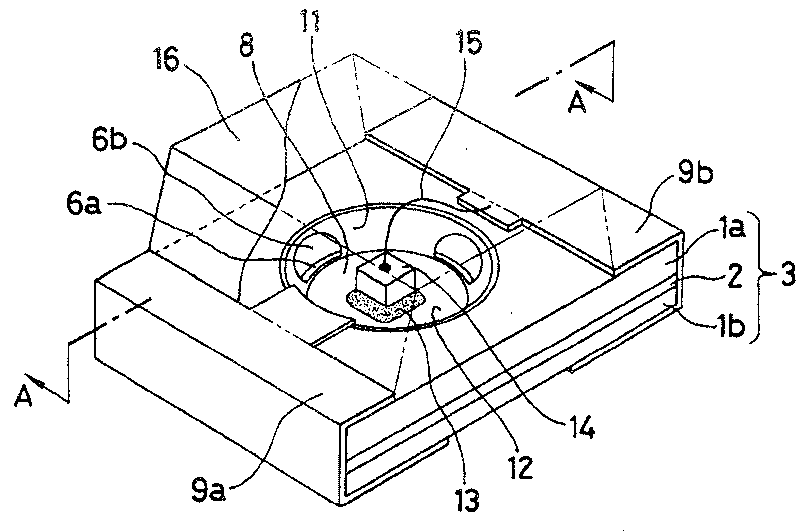
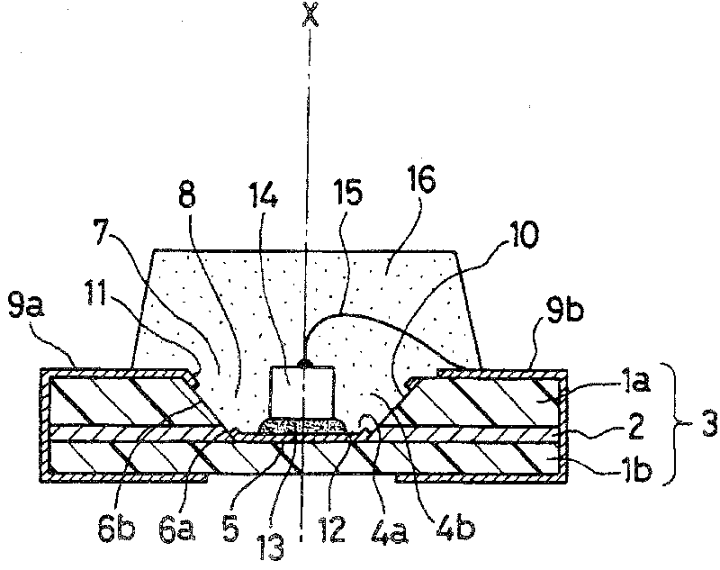
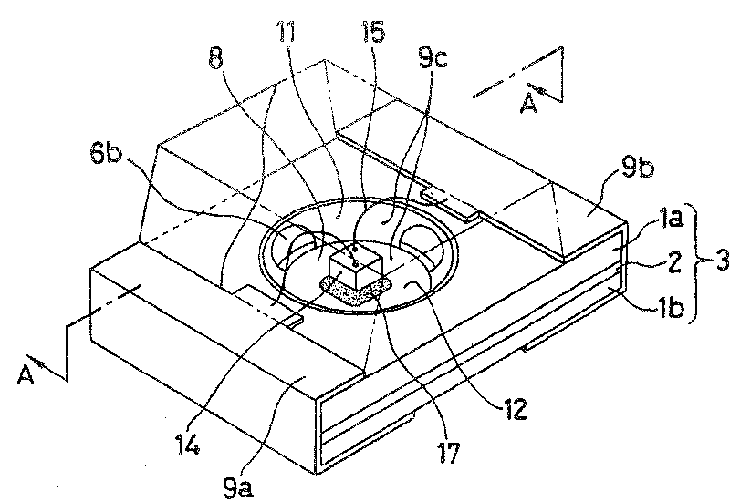
[0027] figure 1 It is a perspective view showing an embodiment of the semiconductor light emitting device of the present invention, figure 2 Yes figure 1 The A-A section diagram.

[0028] The substrate 3 is formed by bonding two insulating substrates 1 a , 1 b with an adhesive sheet 2 interposed therebetween. A substantially circular through-hole 4a is provided in the center of the adhesive sheet 2, and a substantially circular through-ho...


PUM


Abstract

A semiconductor light emitting device is provided. In a traditional semiconductor light emitting device wherein a semiconductor light emitting element fixed on the metal bottom surface in concave of the substrate by bond such as conductive bond is installed by sealing resin, optical property degradation and poor electrical property is generated by the thermal stress of sealing resin under a high temperature packaging environment and a use environment of a large temperature change, and an interfacial delamination between metal bottom surface and the bond. The invention provides a semiconductorlight emitting device with a high reliability which prevents optical property degradation and poor electrical property by partially removing the metal pattern on the inner surface of the concave to expose the insulator on the bottom from the sealing resin, and forming an interface that is of strong binding force with insulator and sealing resin. As a result, it reduces an impact of thermal stressof sealing resin under a high temperature packaging environment and a use environment of a large temperature change which causes the interfacial delamination between the metal bottom surface and the bond.

Description

technical field [0001] The present invention relates to a semiconductor light-emitting device, in particular to a semiconductor light-emitting device in which a semiconductor light-emitting element is mounted inside a recess provided on a substrate and the semiconductor light-emitting element is resin-sealed. Background technique [0002] For semiconductor light-emitting devices, such as Figure 7 and Figure 8 device with the structure shown. Figure 7 is a top view, Figure 8 Yes Figure 7 The A-A section diagram. A pair of circuit patterns 51a, 51b are formed at opposite end portions on the front side of the insulator 50, and each circuit pattern 51a, 51b is formed to wrap around from the edge to the back side through the side surface. In addition, a concave portion 52 is provided at a substantially central portion of the surface side of the insulator 50, and a circuit pattern is formed on the entire surface of the inner bottom surface 53 and the entire inner peripheral...

Claims


Application Information

Patent Timeline
Patent Type & Authority Patents(China)
IPC IPC(8): H01L33/00H01L23/31H01L33/60H01L33/62
CPCH01L2224/48091H01L2224/48465H01L2224/73265H01L2224/48227
Inventor 渡边晴志
Owner STANLEY ELECTRIC CO LTD
Why Eureka
Try Eureka