

Delamination processes and fabrication of thin film devices thereby
a technology of thin film and fabrication process, which is applied in the direction of chemistry apparatus and processes, synthetic resin layered products, other domestic articles, etc., can solve the problems of many desirable flexible substrates, terephthalate, and complicated process
- Summary
- Abstract
- Description
- Claims
- Application Information
AI Technical Summary
Benefits of technology
Problems solved by technology
Method used
Image

Examples
Embodiment Construction
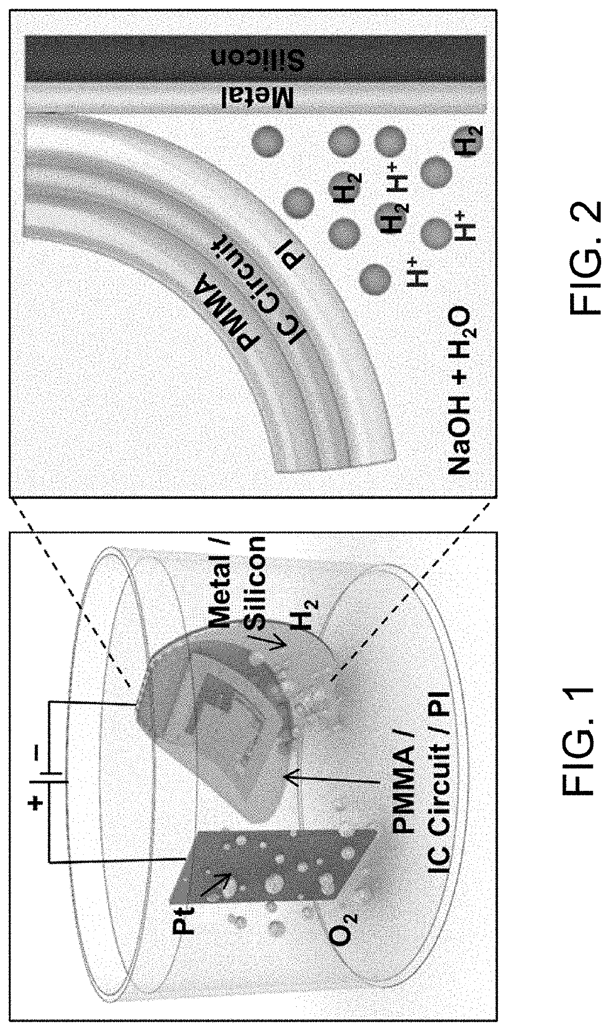
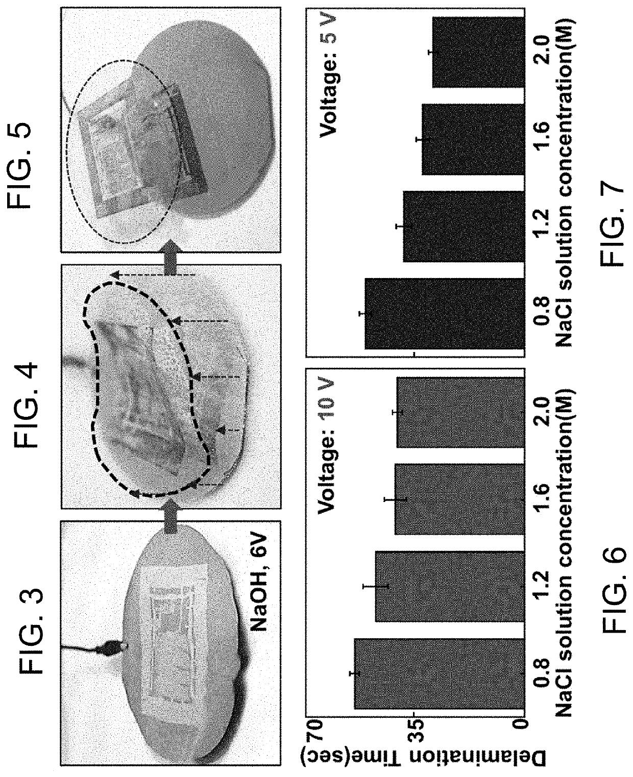
[0023]The following describes interfacial delamination processes that enable the fabrication of thin film devices on a wide variety of surfaces and substrates of interest. The delamination processes are generated by electrochemical reactions at the interface between a pre-fabricated thin film device and a donor / host substrate on which the device was fabricated. The processes can be controlled to facilitate intact separation of relatively large thin film devices from donor / host substrates without the need to use mechanical peeling tools or equipment. The devices may then be transferred to flexible, stretchable, and / or transparent substrates, and yield flexible, stretchable, and / or transparent thin film devices.
[0024]The delamination processes further enable the physical separation of prefabricated thin film devices from a host / donor substrate (e.g., a semiconductor wafer or glass substrate) to enable wafer-scale, defect-free delamination of multiple-stacked thin film devices, and ena...
PUM
| Property | Measurement | Unit |
|---|---|---|
| Molar density | aaaaa | aaaaa |
| Structure | aaaaa | aaaaa |
| Electrical conductor | aaaaa | aaaaa |
Abstract
Description
Claims
Application Information