CMOS symmetrical output D flip-latch with self-correction function

A symmetric output, latch technology, applied in the direction of pulse generation, electrical components, and electrical pulse generation, can solve the problem of not providing CLK-D latch circuit structure, not providing NORSR latch circuit structure, and not having resistance. Soft errors and other problems, to achieve the effect of strong resistance to soft errors

Inactive Publication Date: 2007-04-25
TSINGHUA UNIV
View PDF1 Cites 0 Cited by
  • Summary
  • Abstract
  • Description
  • Claims
  • Application Information

AI Technical Summary

Problems solved by technology

However, this structure is only for the SR latch composed of NAND, and does not provide the circuit structure of the SR latch composed of NOR, let alone the circuit structure of the CLK-D latch.
And more importantly, it does not have the ability to self-correct soft errors

Method used


Image

  • CMOS symmetrical output D flip-latch with self-correction function
  • CMOS symmetrical output D flip-latch with self-correction function
  • CMOS symmetrical output D flip-latch with self-correction function

Examples


Embodiment Construction

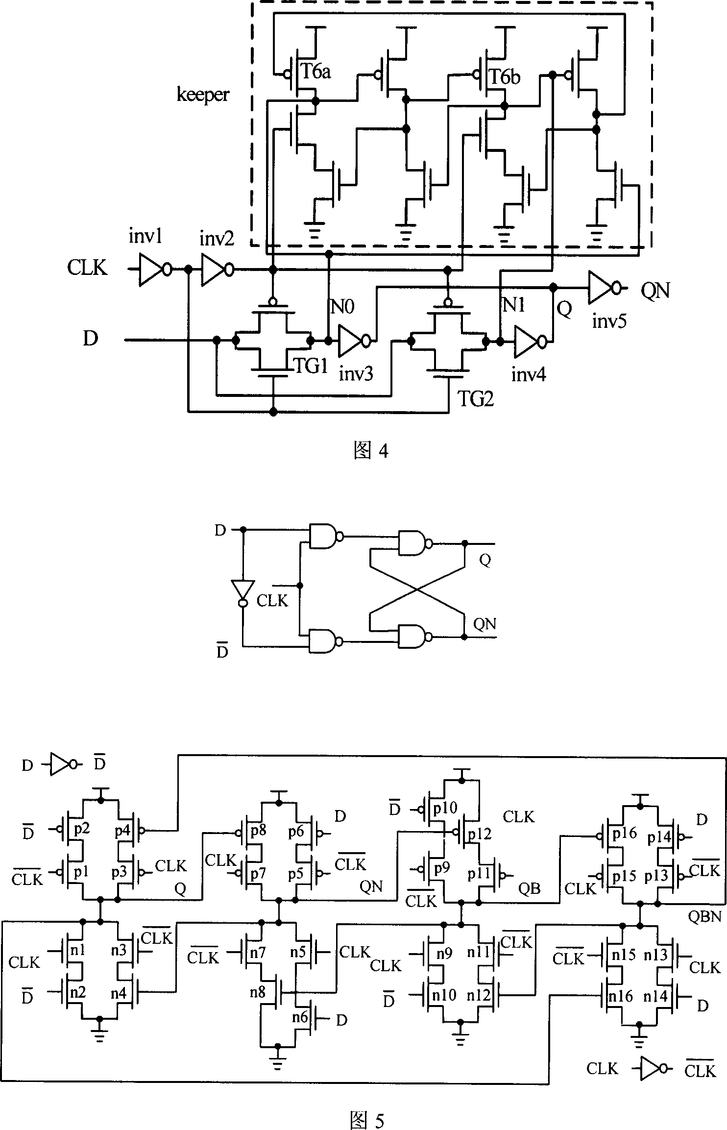
[0018] The technical solution of the present invention to solve the technical problem is: a CMOS symmetrical output D latch with self-correction function controlled by the clock CLK, as shown in FIG. 5 .

[0019] For the CMOS symmetrical output D latch with self-correction function controlled by the clock CLK shown in Figure 5 . When CLK is at low level, n1 and p1 are in cut-off state, p4 and n4 are in conduction state, so the voltage at point Q is in hold state. At the same time, other nodes such as QN, QB, and QNB are also in hold state. When CLK is high, the state of Q depends on the value of D. When D is high, Q is charged through p1 and p2, and QN is discharged through n5 and n6 to realize the function of latching high level. When D is low, Q discharges through n1 and n2, and QN charges through p5 and p6 to realize the function of latching low level.

[0020] It can be seen that in any case there are only two transistors on the charge and discharge branches. Consideri...


PUM


Abstract

The invention relates to a symmetry output register, which is characterized in that the discharge or charge branch with changed state has only two transistors; since the CLK and D signals have one in stable state when another one turnovers, therefore, it has only one transistor in control state when state changes, to accelerate the turnover speed, with better symmetry. Since it has abundant circuit, when two circuits in hold states, it can automatically recover the soft error caused by radios.

Description

technical field [0001] The technical field of direct application of "CMOS symmetrical output D latch with self-correction function" is high-performance integrated circuit design. The proposed circuit is a kind of CMOS symmetrical output latch unit with self-correction function for errors caused by noise, cosmic rays, etc. Background technique [0002] As the CMOS integrated circuit manufacturing process gradually enters the nanoscale field, the scale and complexity of integrated circuits are increasing day by day. Soft errors caused by cosmic ray particle bombardment pose a certain threat to the reliability of integrated circuits. Due to the progress of the process, the node capacitance in the CMOS circuit is reduced, so that the total charge required to make a node flip is reduced, which means that the low-energy cosmic ray particles that would not have an impact in the past will now affect circuit poses enough of a threat. In addition, due to the decrease of the power su...

Claims


Application Information

Patent Timeline
Patent Type & Authority Applications(China)
IPC IPC(8): H03K3/012H03K3/356
Inventor 林赛华杨华中汪蕙
Owner TSINGHUA UNIV
Why Eureka
Try Eureka