

Method and apparatus for operating a string of charge trapping memory cells
A technology of memory unit and charge storage, which is applied in static memory, read-only memory, digital memory information, etc., and can solve serious problems such as the limitation of PHINES structure expansion
Patent Information
- Authority / Receiving Office
- CN · China
- Patent Type
- Applications(China)
- Current Assignee / Owner
- Publication Date
- 2007-06-27
Smart Images
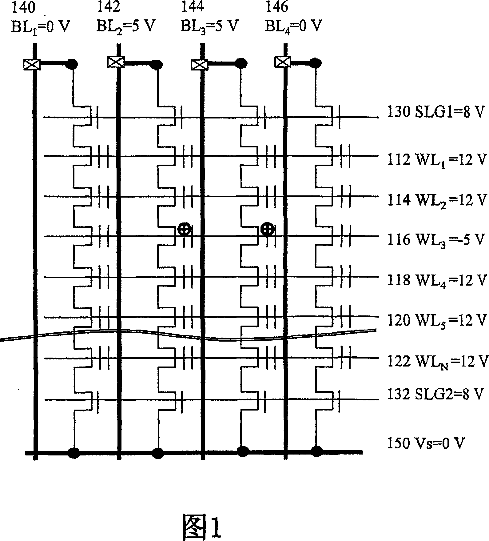
Figure 1 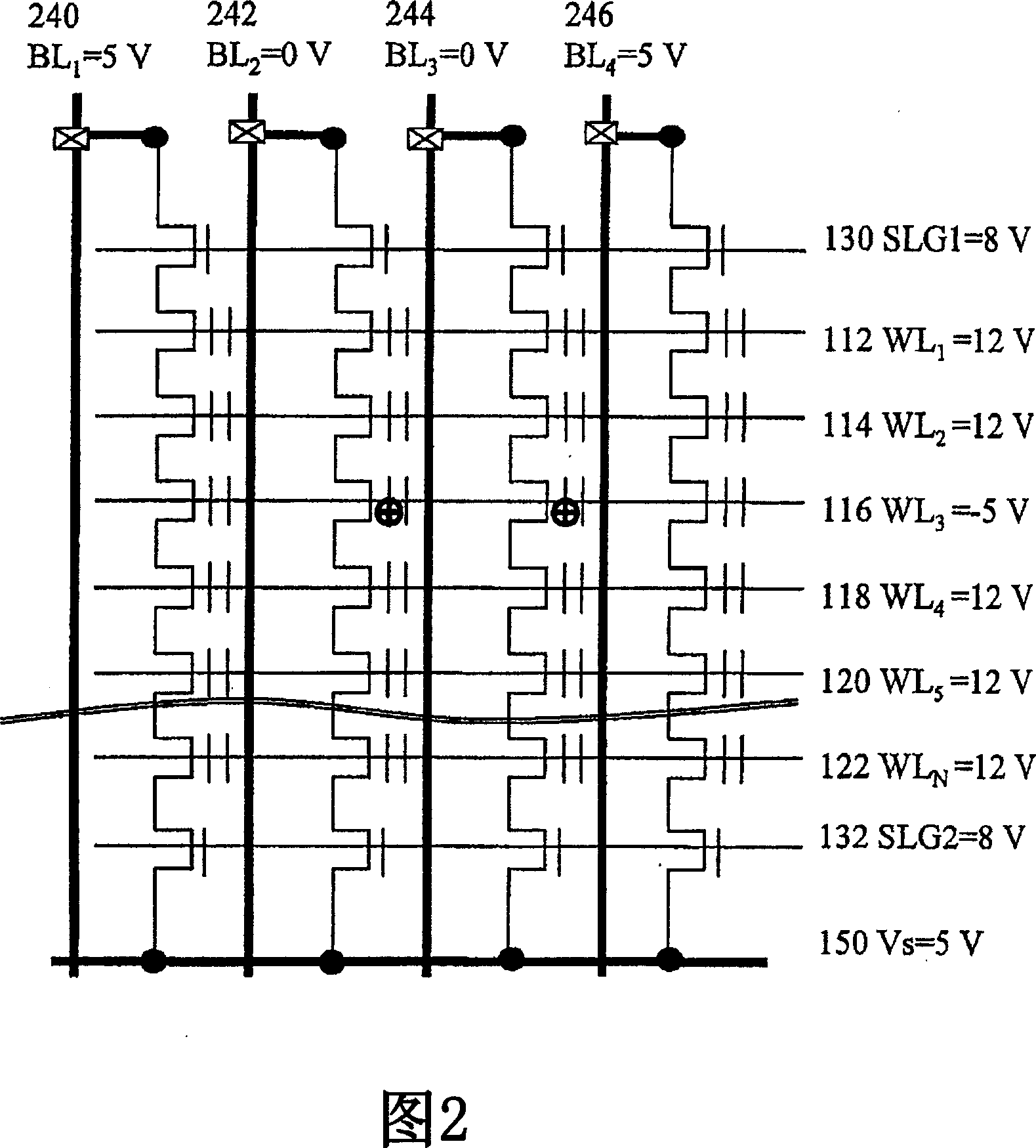
Figure 2 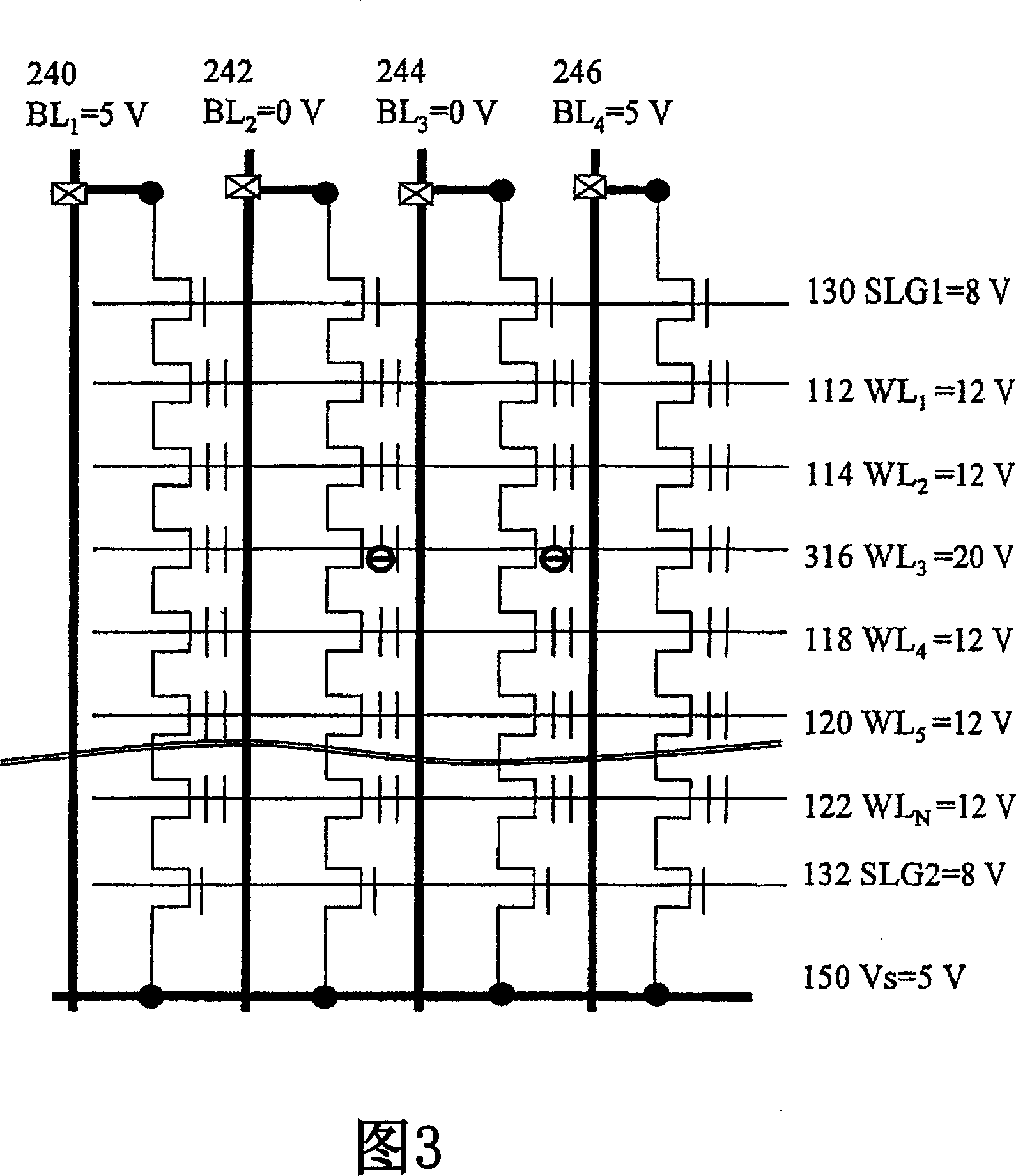
Figure 3
Abstract
Description
technical field
[0001] The present invention relates to electronically programmable and erasable nonvolatile memory, and more particularly to charge trapping memory, each charge trapping memory cell having a limited charge storage state. Background technique
[0002] The electrically programmable and erasable non-volatile memory technology based on the charge storage structure of the known flash memory has been applied in various modern fields. As the size of integrated circuits shrinks, memory cell structures based on charge-trapping dielectric layers are gradually attracting attention because of their mass production and simple manufacturing processes. The memory cell structure mainly based on the charge trapping dielectric layer includes the structure named PHINES in the industry, and these memory cell structures store data by trapping charges in the charge trapping dielectric layer (such as silicon nitride layer). When negative charges are trapped or positive charges ar...
Examples
Embodiment Construction
[0050] Figure 1 shows an array of NAND strings having non-volatile charge-trapping memory cells having at most one single charge storage state programmed with holes. The array shown includes four strings, or columns, of charge-trapping memory cells, each column having a first terminal and a second terminal, the first terminal terminating in a first row select transistor SLG1 with a gate bias of 8 volts. 130, the second terminal is terminated by the second row select transistor SLG2 132 whose gate bias is 8 volts. The contents of the array are accessed through bit lines BL1 140 biased at 0 volts, BL2 142 biased at 5 volts, BL3 144 biased at 5 volts, and BL4 146 biased at 0 volts, each bit line The first terminals of the charge-trapping memory cells of the corresponding columns are connected, and the second terminals of the charge-trapping memory cells of these columns are connected to the voltage source 150 biased at 0 volts. These four columns of charge trapping memory cells ...