

Method and apparatus for operating a non-volatile memory array
- Summary
- Abstract
- Description
- Claims
- Application Information
AI Technical Summary
Benefits of technology
Problems solved by technology
Method used
Image

Examples
Embodiment Construction
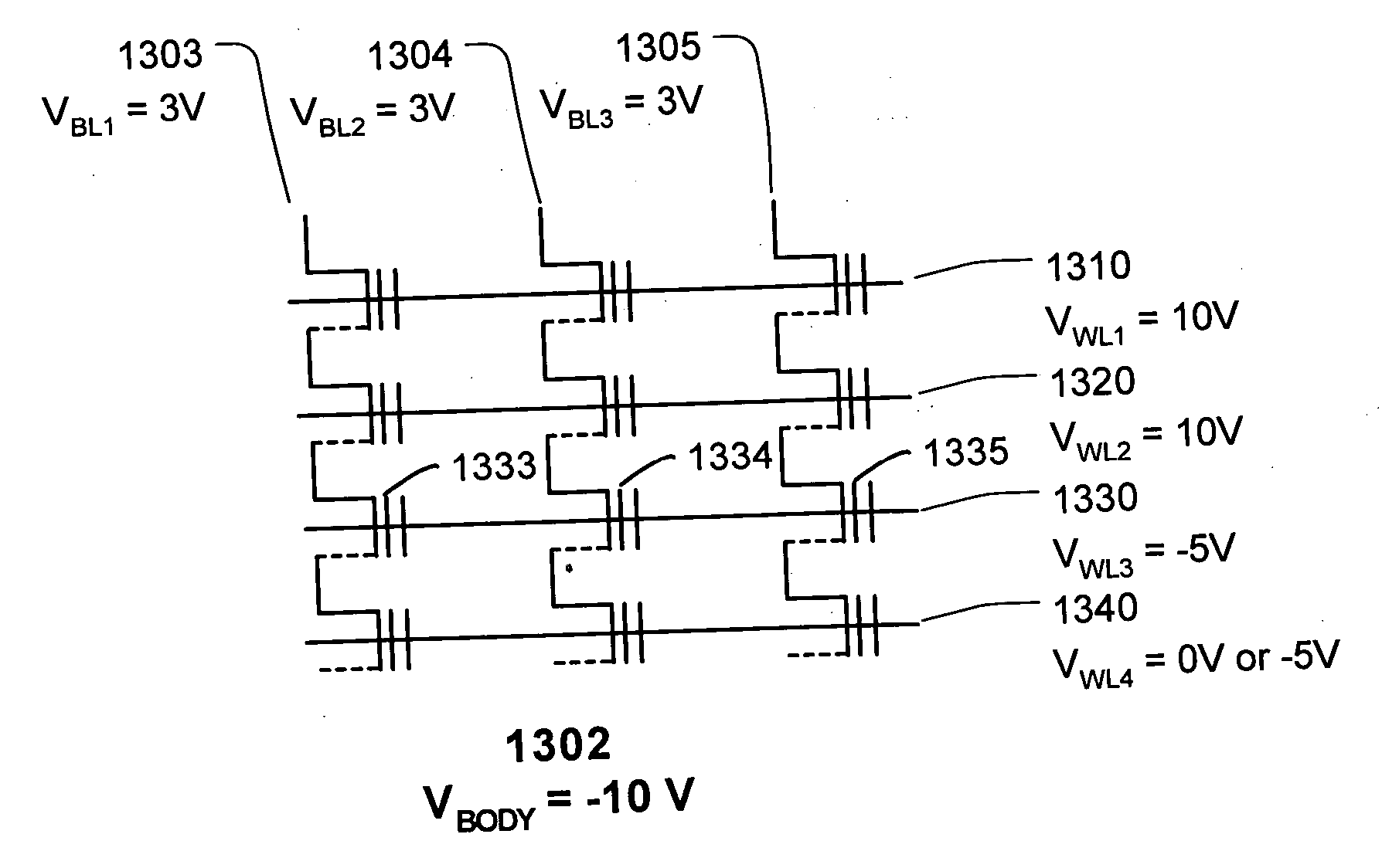
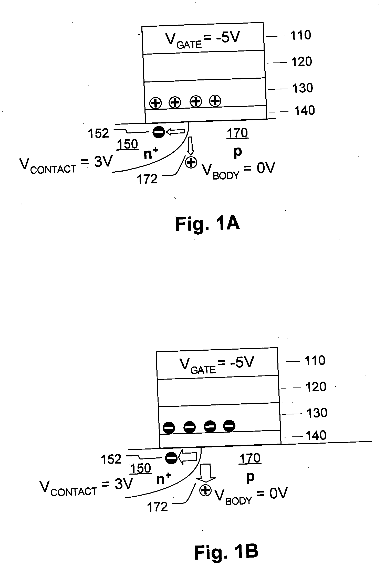
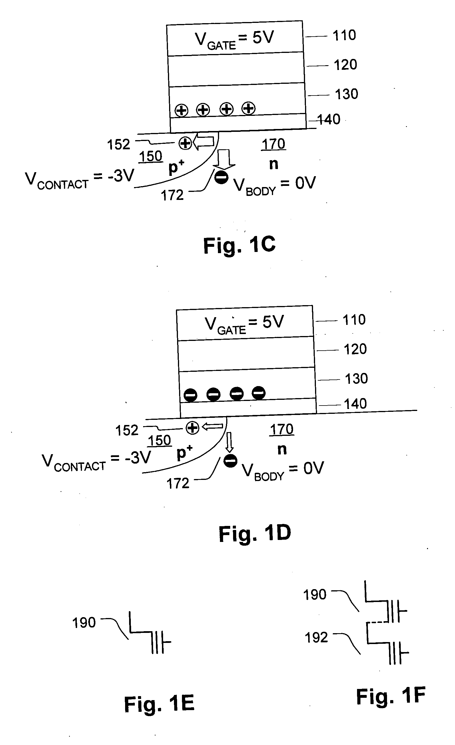
[0056]FIG. 1A and FIG. 1B are simplified diagrams of a charge trapping memory cell, showing a read operation with a negative voltage on the gate being performed on a charge trapping structure. In FIG. 1A, the charge trapping structure has a charge storage state with relatively more net positive charge than in FIG. 1B. The charge trapping memory cell of FIG. 1A and FIG. 1B has a p-doped body region 170 and an n+-doped contact region 150. The remainder of the memory cell includes a bottom dielectric structure 140 (bottom oxide) on the body region 170, a charge trapping structure 130 on he bottom dielectric structure 140, a top dielectric structure 120 (top oxide) on the charge trapping structure 130, and a gate 110 on the oxide structure 120. Representative top dielectrics include silicon dioxide and silicon oxynitride having a thickness of about 5 to 10 nanometers, or other similar high dielectric constant materials, for example Al2O3. Representative bottom dielectrics include silico...
PUM
 Abstract
Description
Claims
Application Information