Filling through-holes

a technology of through-holes and copper plating, which is applied in the direction of liquid/solution decomposition chemical coating, printed element electric connection formation, coating, etc., can solve the problems of copper plating's increased difficulty in filling through-holes, and increased difficulty in forming through-holes. , to achieve the effect of improving throwing power, reducing or inhibiting dimple formation and voids

Inactive Publication Date: 2018-12-11
ROHM & HAAS ELECTRONICS MATERIALS LLC
View PDF26 Cites 0 Cited by
  • Summary
  • Abstract
  • Description
  • Claims
  • Application Information

AI Technical Summary

Benefits of technology

[0009]The methods reduce or inhibit dimple formation and voids during through-hole filling. Dimples are typically less than 10 μm deep. The reduced depth of the dimples and void area improves throwing power, thus providing a substantially uniform copper layer on the surface of the substrate and good through-hole filling. In addition, the methods may be used to fill though-holes of substrates having thickness ranges of 100 μm or greater. The methods also inhibit nodule formation.

Problems solved by technology

Filling the through-holes by copper plating has become more and more difficult with higher aspect ratios.
This results in larger voids and deeper dimples.
Another problem with through-hole filling is the way they tend to fill.
If the right combination of additives is not chosen then the copper plating results in undesired conformal copper deposition.
Often the copper fails to completely fill the through-hole and both ends remain unfilled.
Entire dimple elimination during through-hole filling is rare and unpredictable.
Larger dimples affect further processing of the panel and larger voids affect device performance.
However, this process is both time consuming and inefficient.
Failure to change baths at the correct time typically results in dimple and void formation.
Moreover, using two distinct plating baths for a single process increase the cost to both the manufacture and the customer.
The plating process must be stopped to change the baths, thus further reducing the efficiency of the process.
While conventional direct current plating has been successful in providing acceptable through-hole fill under some circumstances for printed circuit boards having a thickness of 100 μm or less, attempts to fill through-holes in boards with thickness ranges exceeding 100 μm has been less than satisfactory.
Often, the through-holes have unacceptable amounts of dimples exceeding 10 μm in depth and average void areas in the through-holes in excess of 10% to 15%.
Another problem encountered in metal plating is the formation of nodules on the metal deposit.
Nodules are undesirable for a variety of electrical, mechanical, and cosmetic reasons.
For example, nodules are readily detached and carried by cooling air flows into electronic assemblies, both within and external to electronic article housings, where they may cause short-circuit failure.
Such conventional methods leave room for worker error and are inefficient.

Method used


Image

  • Filling through-holes
  • Filling through-holes
  • Filling through-holes

Examples


example 2

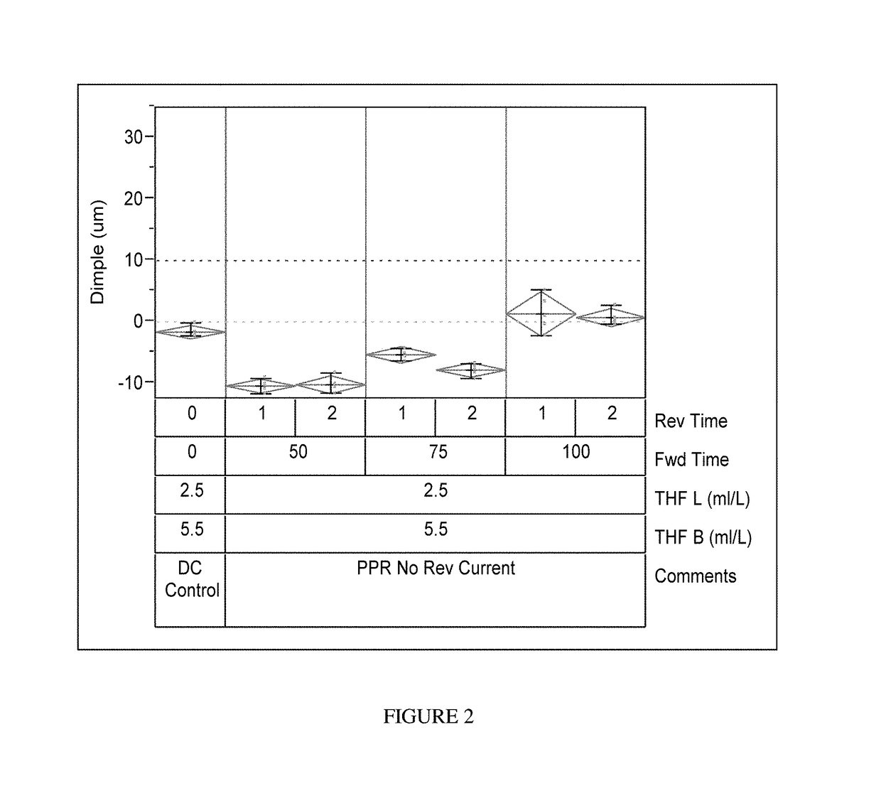
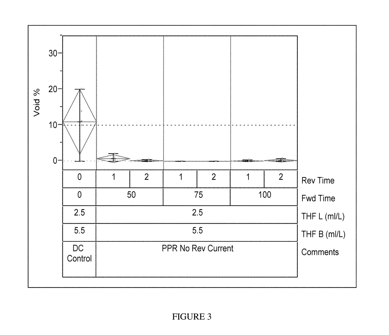
[0038]Six FR4 / glass-epoxy coupons 5 cm wide, 15 cm long and 200 μm thick with a plurality of through-holes were provided by Tech Circuit. The through-holes had an average diameter of 100 μm. The coupons were plated with CIRCUPOSIT™ 880 Electroless Process plating formulation and method (available from Dow Electronic Materials, Marlborough, Mass.) to form a copper layer on one side of the coupon and on the walls of the through-holes. The thickness of the copper layer on each coupon was 0.3 μm. The coupons were pre-cleaned using a conventional copper cleaner. The coupons were then placed in Haring cells which contained a copper electroplating bath with a formula as shown in Table 1 above.

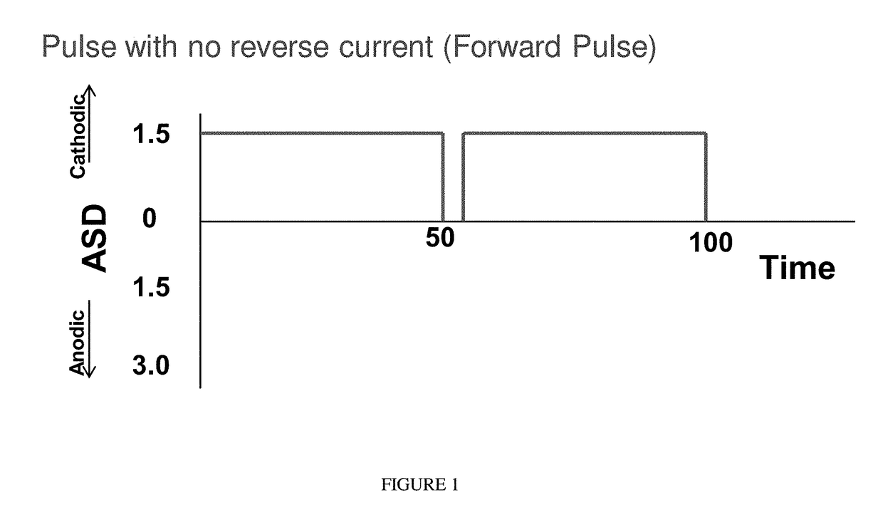
[0039]The coupons were connected to a conventional DC rectifier. The counter electrodes in the Haring cells were insoluble anodes. The plating baths were air agitated during electroplating at 2.4 L / minute. Plating was done at room temperature. The current density was set at 1.5 ASD. Two of the coupons...

example 3

[0041]The method described in Example 2 was repeated using four FR4 / glass-epoxy coupons 5 cm wide, 15 cm long and 200 μm thick with through-holes having an average diameter of 100 μm. The forward pulse time was either 20 ms or 35 ms and the interruption times were either 1 ms or 2 ms. There was no reverse current. The coupons were sectioned and analyzed for dimple size and percent void area as described in Example 2 above. The coupons which were plated at a forward current density for 20 ms with 1 ms current interruptions had an average dimple size of 4.3 μm and the coupons with current interruptions of 2 ms had an average dimple size of 5.4 μm. The coupons which were plated with a forward current density for 35 ms with 1 ms interruptions had an average dimple size of −2.78 and the coupons with the 2 ms interruptions had an average dimple size of 6.67. All of the through-holes analyzed all fell below 10 μm. None of the coupons analyzed showed voids. Also, no nodules were observed.


PUM

PropertyMeasurementUnit
thickaaaaaaaaaa
thickaaaaaaaaaa
diametersaaaaaaaaaa

Abstract

Pulse plating methods which include a forward pulse but no reverse pulse inhibit or reduce dimpling and voids during copper electroplating of through-holes in substrates such as printed circuit boards. The pulse plating methods may be used to fill through-holes with copper where the through-holes are coated with electroless copper or flash copper.

Description

FIELD OF THE INVENTION[0001]The present invention is directed to a method of filling through-holes. More specifically, the present invention is directed to a method of filling through-holes using a pulse plating method with forward pulse and no reverse pulse.BACKGROUND OF THE INVENTION[0002]High density interconnects is an important design in the fabrication of printed circuit boards with through-holes. Miniaturization of these devices relies on a combination of thinner core materials, reduced line widths and smaller diameter through-holes. The diameters of the through-holes range from 75 μm to 200 μm. Filling the through-holes by copper plating has become more and more difficult with higher aspect ratios. This results in larger voids and deeper dimples. Another problem with through-hole filling is the way they tend to fill. Unlike vias which are closed at one end through-holes pass through a substrate and are open at two ends. Vias fill from bottom to top. In contrast, when through...

Claims


Application Information

Patent Timeline
Patent Type & Authority Patents(United States)
IPC IPC(8): H05K3/42C25D5/18C25D7/00C25D3/38C23C18/16
CPCH05K3/424C25D5/18C25D7/00H05K3/423H05K2203/1492C23C18/1653C25D3/38H05K2201/09563H05K2203/0723C25D5/627
Inventor JAYARAJU, NAGARAJANBARSTAD, LEON R.NAJJAR, ELIE H.
Owner ROHM & HAAS ELECTRONICS MATERIALS LLC
Why Eureka
Try Eureka