Texturing of monocrystalline semiconductor substrates to reduce incident light reflectance

a monocrystalline semiconductor and incident light reflectance technology, applied in the field of texturing monocrystalline semiconductor substrates, can solve the problems of high reflectivity, unsatisfactory low boiling point and low flash point, toxicity to workers, etc., to reduce the formation of flat areas, improve the efficiency of devices, and increase the effect of incident light absorption

Active Publication Date: 2014-07-01
SUN CHEM CORP
View PDF7 Cites 0 Cited by
  • Summary
  • Abstract
  • Description
  • Claims
  • Application Information

AI Technical Summary

Benefits of technology

[0007]The methods and compositions are used to anisotropically texture monocrystalline semiconductors for photovoltaic devices, including semiconductors in the manufacture of solar cells. The addition of one or more of hydantoin and hydantoin derivatives in combination with one or more alkoxylated glycols inhibit or reduce formation of flat areas between pyramid structures on the textured monocrystalline semiconductors to increase incident light absorption and improve the efficiency of the devices. In addition, the hydantoin compounds improve the efficiency of the texturing method.

Problems solved by technology

Alkali hydroxides by themselves produce unevenly textured surfaces which result in areas of high reflectivity.
Solutions of hydrazine or ethylene diamine or pyrocatechol can be used instead of alkali hydroxides but they are disadvantageous on account of their toxicity to workers.
Although isopropanol is included in many conventional texturing compositions, its low boiling point and low flash point are undesirable properties for texturing compositions.

Method used


Image

  • Texturing of monocrystalline semiconductor substrates to reduce incident light reflectance
  • Texturing of monocrystalline semiconductor substrates to reduce incident light reflectance
  • Texturing of monocrystalline semiconductor substrates to reduce incident light reflectance

Examples


example 1

[0061]Two doped monocrystalline silicon semiconductor wafers (obtained from SolarGiga) having n+ doped zones on the front side or emitter layer and a pn-junction below the emitter layer were textured with one of the two texturing solutions shown in Table 1.

[0062]

TABLE 1ComponentSolution 1Solution 2Tripropylene glycol12 wt %2 wt %Potassium hydroxide6 wt % (25 g / L)6 wt % (25 g / L)1,4-butanediol22 wt %2 wt %N-isopropylhydroxylamine30.1 wt %  0.1 wt %  Hydantoin400.05 wt %  WaterBalanceBalance1weight average molecular weight = 192 g / mole, flash point = 140.5° C., Boiling point = 268° C.;2Flash point = 121° C.;3Hydroguard ™ I-15 (available from The Dow Chemical Company, Midland, MI);4melting point = 221-223° C. (Decomposes).

[0063]Each wafer was immersed in one of the two texturing solutions for 10 minutes. The solutions were kept at 80° C. and the pH of the solutions was at 13 measured with a conventional laboratory pH meter.

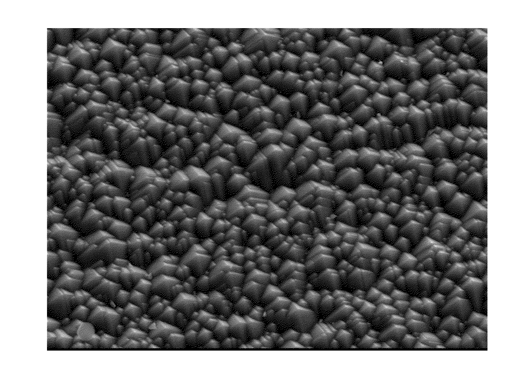
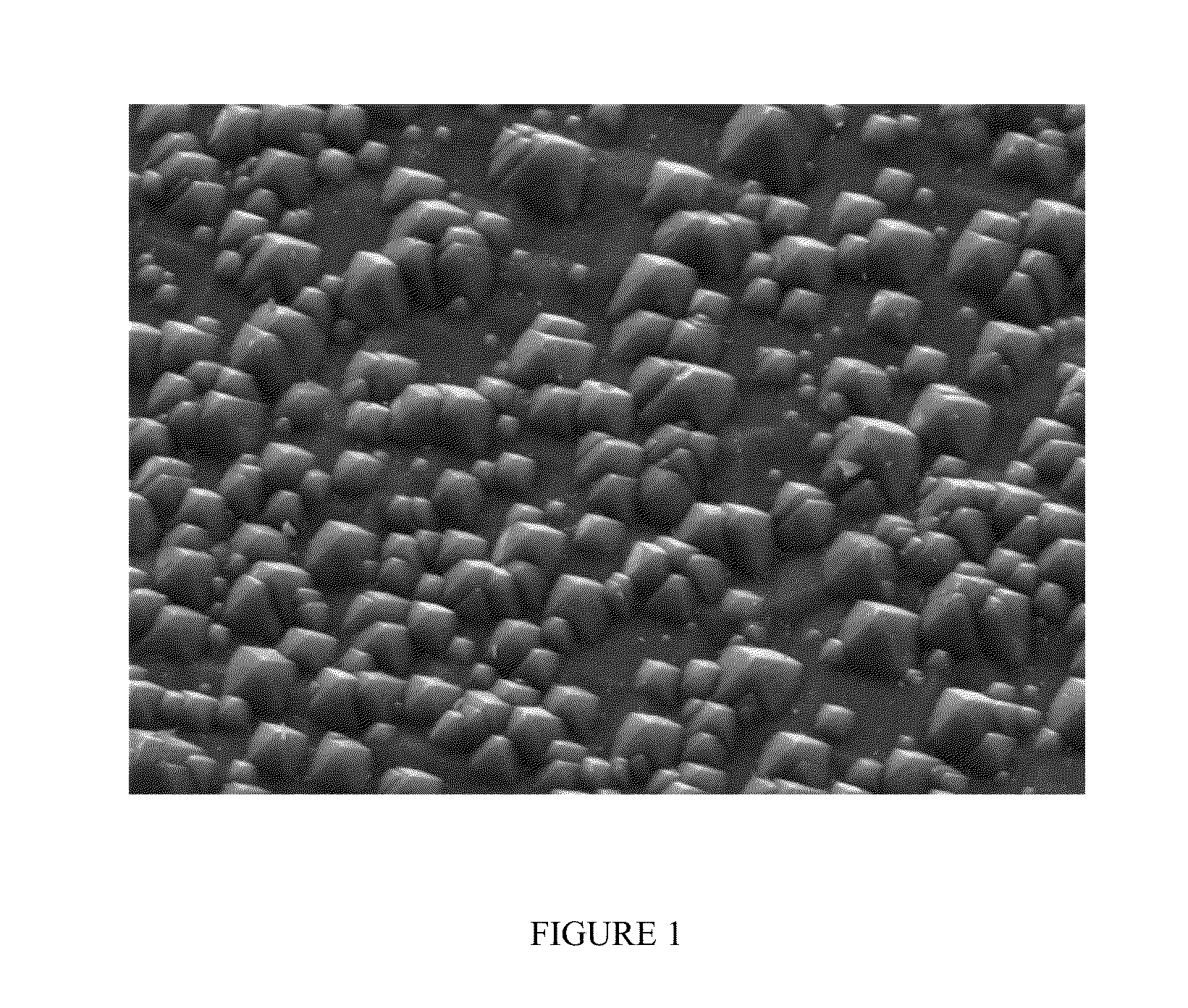
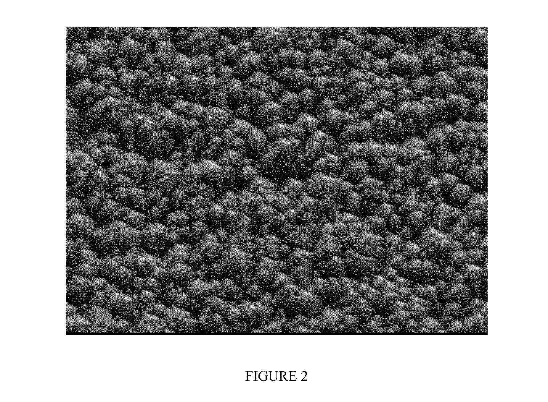
[0064]FIG. 1 is a SEM of the wafer textured with solution 1 take...

examples 2-5

Controls

[0065]Four aqueous based texturing solutions were made as shown in Table 2 below. Four monocrystalline silicon semiconductor wafers (obtained from SolarGiga) having n+ doped zones on the front side or emitter layer and a pn-junction below the emitter layer were weighed using a conventional laboratory balance. Each wafer was then immersed in one of the four texturing solutions for 30 minutes at 75° C. The pH of the texturing solutions was 13. The wafers were then removed from their respective texturing solutions, rinsed with water and air dried. Each wafer was then weighed and the amount of silicon etched per side was determined as shown in Table 2 below.

[0066]Reflectance of the textured surface was determined using a MacBeth Coloreye Reflectometer 7000 at the wavelength of 600 nm The source of the incident light was a pulsed xenon bulb. An average of 6 reflectance readings was taken across the surface of each wafer. The average reflectance is shown in Table 2.

[0067]

TABLE 2AD...

examples 6-7

Controls

[0069]Two aqueous based texturing solutions were made as shown in Table 3 below. Two monocrystalline silicon semiconductor wafers (obtained from SolarGiga) having n+ doped zones on the front side or emitter layer and a pn-junctions below the emitter layer were weighed using a conventional laboratory balance. Each wafer was then immersed in one of the two texturing solutions for 30 minutes at 75° C. The wafers were then removed from their respective texturing solutions, rinsed with water and air dried. Each wafer was then weighed and the amount of silicon etched per side was determined as shown in Table 3 below.

[0070]Reflectance of the textured surface was determined using the MacBeth Coloreye Reflectometer 7000 at the wavelength of 600 nm. An average of 6 reflectance readings was taken across the surface of each wafer. The average reflectance is shown in Table 3.

[0071]

TABLE 3ADDITIVESODIUM(ExamplesHYDROXIDEADDITIVETIMETEMPERATUREETCH / SIDEREFLECTANCE6-7)(g / L)(wt %)(minutes)(°...


PUM

PropertyMeasurementUnit
boiling pointaaaaaaaaaa
angleaaaaaaaaaa
melting pointsaaaaaaaaaa

Abstract

Monocrystalline semiconductor substrates are textured with alkaline solutions to form pyramid structures on their surfaces to reduce incident light reflectance and improve light absorption of the wafers. The alkaline baths include hydantoin compounds and derivatives thereof in combination with alkoxylated glycols to inhibit the formation of flat areas between pyramid structures to improve the light absorption.

Description

FIELD OF THE INVENTION[0001]The present invention is directed to a method of texturing monocrystalline semiconductor substrates in alkaline baths to reduce incident light reflectance. More specifically, the present invention is directed to a method of texturing monocrystalline semiconductor substrates in alkaline baths which include hydantoin or hydantoin derivatives in combination with alkoxylated glycols to reduce incident light reflectance.BACKGROUND OF THE INVENTION[0002]A textured semiconductor surface reduces reflection across wide bands of incident light thereby increasing absorbed light intensity. Such semiconductors may be used in the manufacture of solar cells. Solar cells are devices that convert light energy incident on their surfaces such as sunlight into electric energy. Reducing the reflectance of light incident on the surface improves conversion efficiency into electric energy. Texturing, however, is not restricted to semiconductors in the manufacture of solar cells ...

Claims


Application Information

Patent Timeline
Patent Type & Authority Patents(United States)
IPC IPC(8): B44C1/22
CPCH01L31/02363Y02E10/52G02B1/111C09K13/06A01N35/08A01N43/28C07D275/04C09K13/00C09K13/02C23C18/38C23C18/40Y02E10/50H01L31/0236H01L31/042H01L31/18
Inventor TOBEN, MICHAEL P.BARR, ROBERT K.O'CONNOR, COREY
Owner SUN CHEM CORP
Why Eureka
Try Eureka