Inter facial architecture for nanostructured optoelectronic devices

a technology of optoelectronic devices and nanostructured active layers, which is applied in the field of optoelectronic devices with nanostructured active layers, can solve the problems of limiting the efficiency of pv devices and lacking random blends in order, and achieves the effect of low cos

Inactive Publication Date: 2009-03-31
AERIS CAPITAL SUSTAINABLE IP
View PDF53 Cites 61 Cited by
  • Summary
  • Abstract
  • Description
  • Claims
  • Application Information

AI Technical Summary

Benefits of technology

[0010]Embodiments of the present invention provide more efficient optoelectron

Problems solved by technology

Unfortunately, electrons and holes can recombine before they are collected, which tends t

Method used


Image

  • Inter facial architecture for nanostructured optoelectronic devices
  • Inter facial architecture for nanostructured optoelectronic devices
  • Inter facial architecture for nanostructured optoelectronic devices

Examples


Embodiment Construction

Contents

I. Glossary

II. General Overview

III. Optoelectronic Apparatus

IV. Optoelectronic Apparatus Fabrication

VI. Conclusion

I. GLOSSARY

[0017]The following terms are intended to have the following general meanings as they are used herein:

[0018]Aspect Ratio: refers to the ratio of diameter to height or depth.

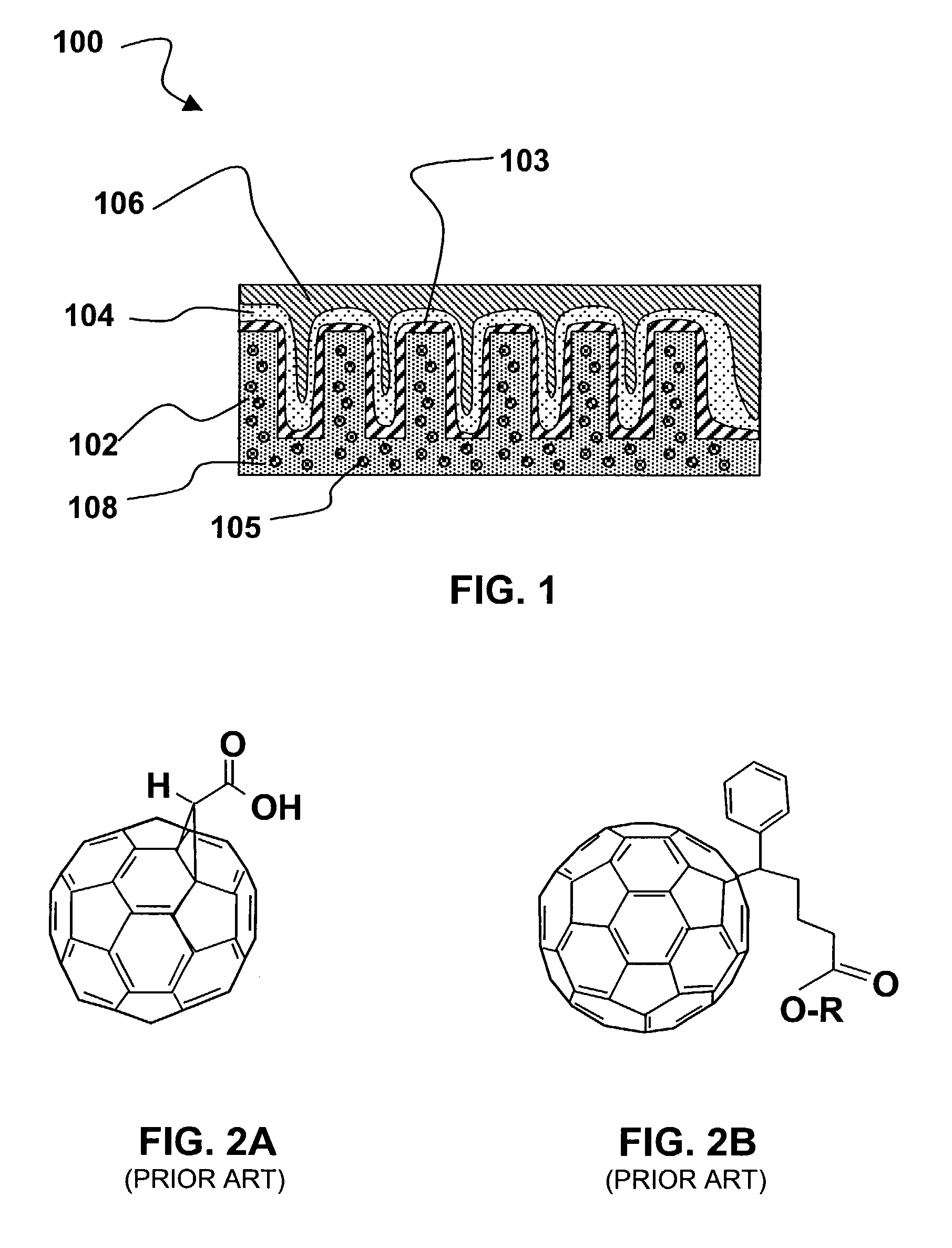
[0019]Buckminsterfullerene: is a molecule having a network of carbon atoms in a closed cage structure. Because of its soccer-ball-like shape, the buckminsterfullerene molecule is often referred to as a “buckyball.” Molecules of this type are also known generally as fullerenes.

[0020]Complementary charge-transfer properties: As used herein, a first and second semiconductor or conductor materials are said to have complementary charge-transfer properties with respect to each other when the first material is a hole-acceptor and / or hole-transporter with respect to the second and the second is an electron-acceptor and / or electron-transporter with respect to the first or vice versa.

[0021]De...


PUM


Abstract

An optoelectronic apparatus, a method for making the apparatus, and the use of the apparatus in an optoelectronic device are disclosed. The apparatus may include an active layer having a nanostructured network layer with a network of regularly spaced structures with spaces between neighboring structures. One or more network-filling materials are disposed in the spaces. At least one of the network-filling materials has complementary charge transfer properties with respect to the nanostructured network layer. An interfacial layer, configured to enhance an efficiency of the active layer, is disposed between the nanostructured network layer and the network-filling materials. The interfacial layer may be configured to provide (a) charge transfer between the two materials that exhibits different rates for forward versus backward transport; (b) differential light absorption to extend a range of wavelengths that the active layer can absorb; or (c) enhanced light absorption, which may be coupled with charge injection.

Description

CROSS-REFERENCE TO AN EARLIER FILED APPLICATION[0001]This application is related to U.S. patent application Ser. Nos. 10 / 290,119, 10 / 303,665 and 10 / 319,406, the entire disclosures of which are incorporated herein by reference.FIELD OF THE INVENTION[0002]This invention relates to optoelectronic devices and more particularly to optoelectronic devices with nanostructured active layers.BACKGROUND OF THE INVENTION[0003]Optoelectronic devices interact with radiation and electric current. Such devices can be light-emitting devices that produce radiation as a result of an applied electric voltage / current or photovoltaic (PV) devices, e.g., solar cells that produce an electric voltage / current as a result of applied radiation. Optoelectronic devices typically one or more active layers of photoactive material sandwiched between two electrodes. At least one of the electrodes is transparent. The active layer typically includes two materials exhibiting complementary charge transfer (e.g., one is ...

Claims


Application Information

Patent Timeline
IPC IPC(8): H01L31/00
CPCB82Y10/00H01L51/0014H01L51/424H01L51/447H01L51/0047Y02E10/549Y02P70/50H10K71/20H10K85/215H10K30/20H10K30/87
Inventor ROSCHEISEN, MARTIN R.SAGER, BRIAN M.PETRITSCH, KLAUSFIDANZA, JACQUELINE
Owner AERIS CAPITAL SUSTAINABLE IP
Why Eureka
Try Eureka