Power converter

a power converter and power conversion technology, applied in the direction of cooling/ventilation/heating modification, semiconductor/solid-state device details, semiconductor devices, etc., can solve the problems of difficult downsizing of the power converter, deteriorating power conversion efficiency, and troublesome connection between the semiconductor module and the control board

Active Publication Date: 2012-07-26
MITSUBISHI ELECTRIC CORP
View PDF12 Cites 57 Cited by
  • Summary
  • Abstract
  • Description
  • Claims
  • Application Information

AI Technical Summary

Benefits of technology

[0021]Further, the current detector originally has terminals because the connection of the control board and the signal line is required. When the number of terminals is increased, and the terminals pene...

Problems solved by technology

However, when the semiconductor module is divided and arranged on both surfaces of the cooler, a connection between the semiconductor module and a control board is problematic.
Therefore, a smoothing capacitor connected to the input wirings cannot come close to the semiconductor modules.
In this case, because the switching loss generated in the semiconductor element, that is, heating of the element becomes large, there arises such a problem that a large-sized cooler needs to be provided, or the power conversion efficiency is deteriorated.
However, a space in which the snubber circuit is mounted is required, and it is difficult to downsize the power converter.
However, this method suffers from such a problem that the performance of the power converter is sacrificed.
As a result, there arises such a problem that it is difficult to downsize the power converter.
Also, the signal transmission distance between the control boards is long, and the influence of the noise is liable to occur.
Therefore, even if the signal transmission speed between the control boards is sacrificed, that is, the performance of the power converter is sacrificed, measures that a filter is used for noise removal are required.
However, because the connector and the signal harness are used, a space in which the connector is arranged, and a space for pulling the harness are required, resulting in such problems that it is difficult to downsize the power converter, and the assembling property is sacrificed by pulling the harness in a small space for downsizing.
However, the complicated lead pin is guided, a fixed structure is required, and it is difficult to curve the ...

Method used


Image

  • Power converter
  • Power converter
  • Power converter

Examples


first embodiment

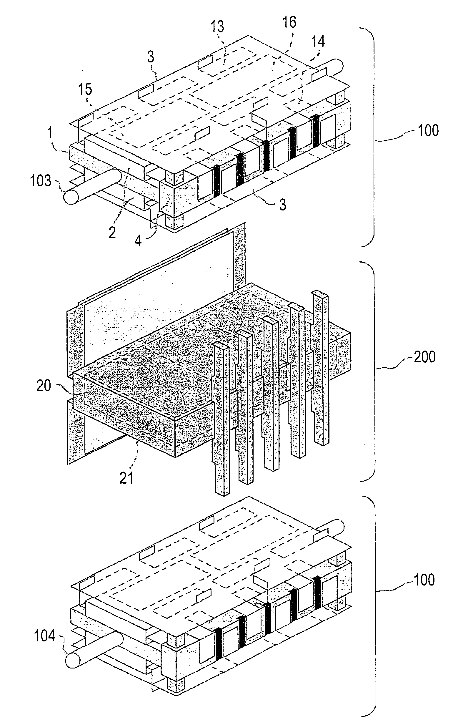
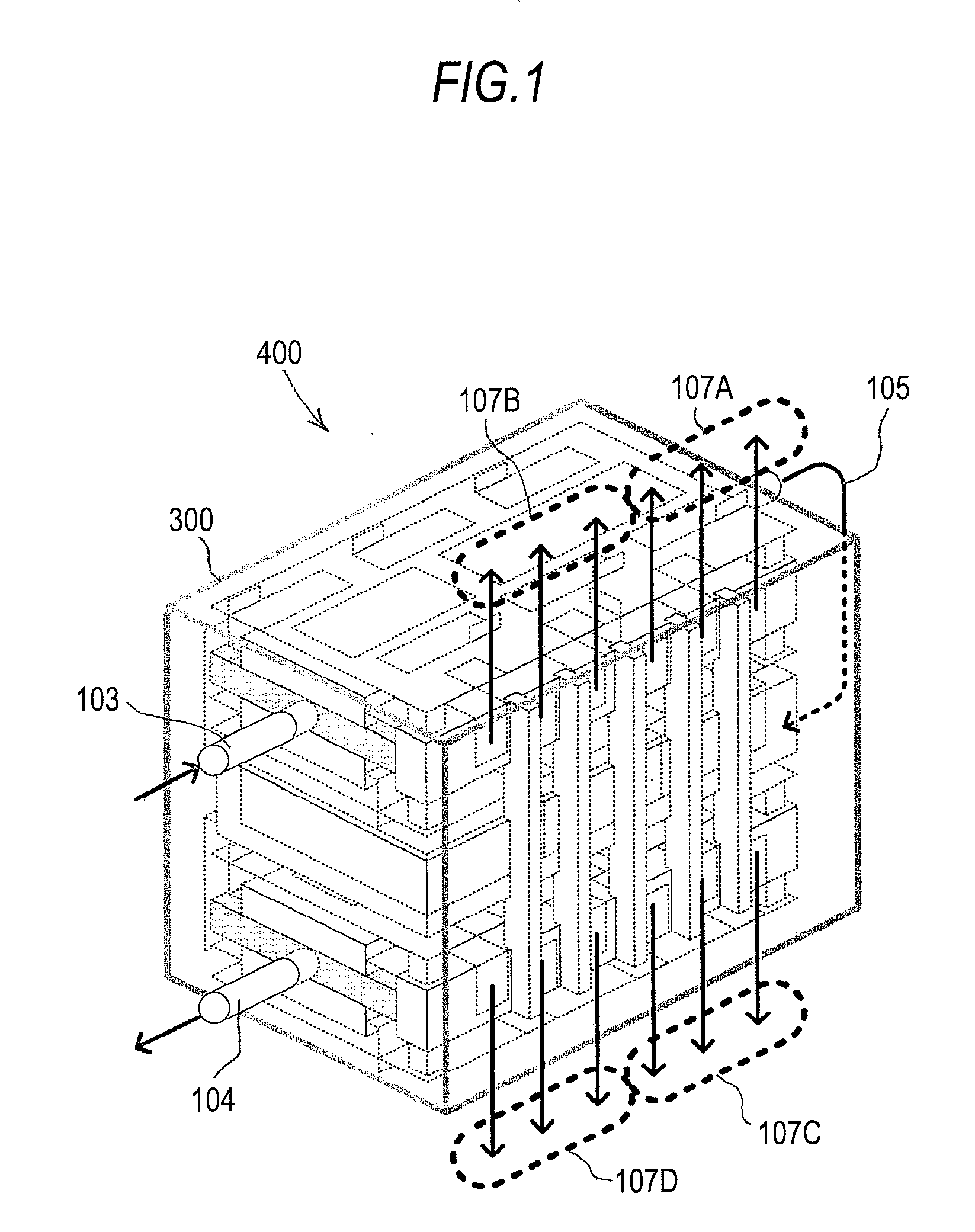
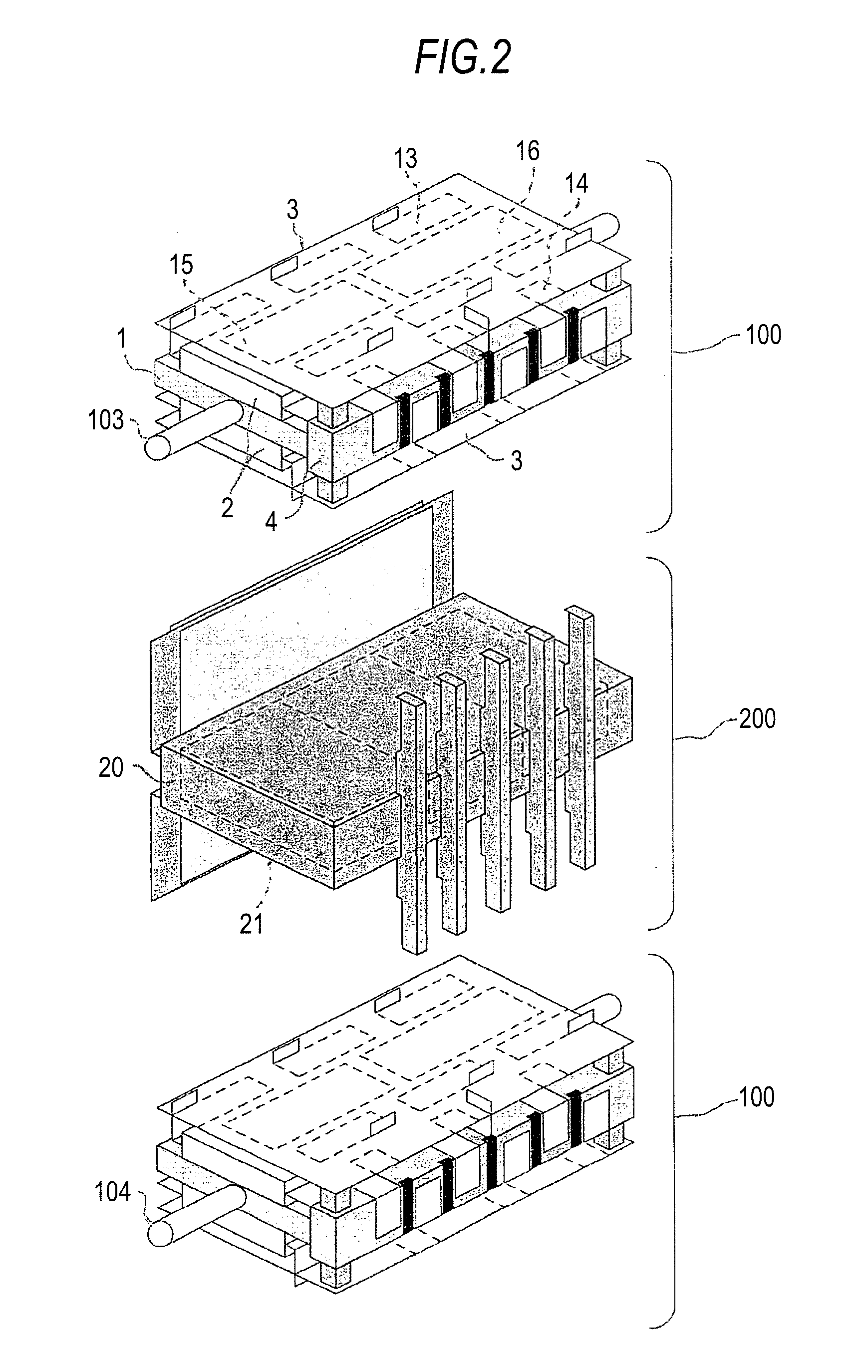
[0065]An overall configuration according to a first embodiment of the invention will be described with reference to FIGS. 1 and 2. In a power converter 400 according to a first embodiment, one power assembly (ASSY) 100 is disposed on each surface of a smoothing capacitor unit 200, and housed in a housing 300. In the power assembly (ASSY) 100, three semiconductor modules 2 and one control board 3 are placed on each surface of a cooler 1. The power converter having four three-phase orthogonal power conversion functions is configured by the 12 semiconductor modules 2, the two coolers 1, the four control boards 3, and the one smoothing capacitor unit 200 in total. First to fourth three-phase outputs 107A, 107B, 107C, and 107D are led from the power converter. Each of the coolers 1 is provided with a cooling water inlet 103, and a cooling water outlet 104 connected to the cooling water inlet 103 through a U-turn flow passage 105.

[0066]A detailed basic configuration of the power assembly ...

second embodiment

[0091]The entire configuration according to a second embodiment of the invention is illustrated in FIGS. 18 and 19. A power converter 400 according to the second embodiment is configured to arrange the smoothing capacitor unit 200 on one side of the power assembly 100 housed in a housing 300. The power converter 400 includes a DC input 101, a three-phase output 107, a cooling water inlet 103, and a cooling water outlet 104. This embodiment exemplifies the power converter having only one large-capacity three-phase orthogonal power conversion function based on the power assembly of the first embodiment. A description will be given of a configuration that the large-capacity power conversion function is realized on the basis of the layout of the smoothing capacitor unit and the power assembly of the first embodiment when only one power assembly is provided.

[0092]A basic configuration of the power converter according to the second embodiment of the invention will be described with refere...

third embodiment

[0113]Subsequently, a configuration according to a third embodiment of the invention will be described. The power converter according to the third embodiment is an example in which the switching element mounted on the semiconductor module according to the second embodiment is replaced with a wideband gap element. In the wideband gap element such as SiC, because the high temperature operation and the high speed switching are enabled, the heat resistance and the noise resistance of the peripheral parts are problematic. In this embodiment, a configuration for improving the heat resistance and the noise resistance of the peripheral parts will be described on the basis of the power converter according to the second embodiment. This embodiment is applied to not only the wideband gap element, but also the power converter according to the first and second embodiments.

[0114]The basic configuration according to the third embodiment of the invention will be described with reference to FIGS. 35...


PUM


Abstract

In a power converter in which semiconductor modules are arranged on both surfaces of a cooler for downsizing, an excellent connection between control boards and a low inductance connection between smoothing capacitors and the semiconductor modules are performed at the same time. The semiconductor modules are disposed on both surfaces of the cooler, and control boards that control the semiconductor modules are arranged opposite to the respective semiconductor modules. The semiconductor modules and the cooler are held between the control boards. A current detector or a terminal block is disposed at a position perpendicular to a surface on which the cooler and the semiconductor modules contact each other, opposite to the cooler. The respective control boards disposed on both surfaces of the cooler are electrically connected by using wirings provided in the current detector or the terminal block.

Description

BACKGROUND OF THE INVENTION[0001]1. Field of the Invention[0002]The present invention relates to a power converter such as an inverter using a semiconductor module.[0003]2. Description of the Related Art[0004]An occupied floor area can be downsized by arranging a semiconductor module on both surfaces of a cooler rather than a case in which the semiconductor module is arranged on only one surface thereof. However, when the semiconductor module is divided and arranged on both surfaces of the cooler, a connection between the semiconductor module and a control board is problematic. For example, in order to control the operation of a plurality of semiconductor modules synchronously, it is desirable to control the semiconductor module by one control board. In order to achieve this, as disclosed in JP-A-2005-73374, control terminals extend in parallel to surfaces of the cooler on which the semiconductor modules are mounted, and the control board is so arranged to face another surface of th...

Claims


Application Information

Patent Timeline
IPC IPC(8): H05K7/20
CPCH02M7/003H01L2924/0002H01L2924/00H01L23/473H01L23/642H01L25/117H05K7/209
Inventor ISHIBASHI, SATOSHIWATANABE, TOSHIOIDENOUE, SHINSUKE
Owner MITSUBISHI ELECTRIC CORP
Why Eureka
Try Eureka