Audio amplifier using multi-level pulse width modulation

a multi-level pulse width modulation and audio amplifier technology, applied in the direction of low-frequency amplifiers, electrical transducers, transducer casings/cabinets/supports, etc., can solve the problems of poor power efficiency at such small audio input signals, poor low-frequency power efficiency, and low-frequency power consumption, so as to reduce the breakdown voltage requirements of semiconductor switches, the effect of robustness and low-cos

Active Publication Date: 2013-08-29
INFINEON TECH AUSTRIA AG
View PDF4 Cites 75 Cited by
  • Summary
  • Abstract
  • Description
  • Claims
  • Application Information

AI Technical Summary

Benefits of technology

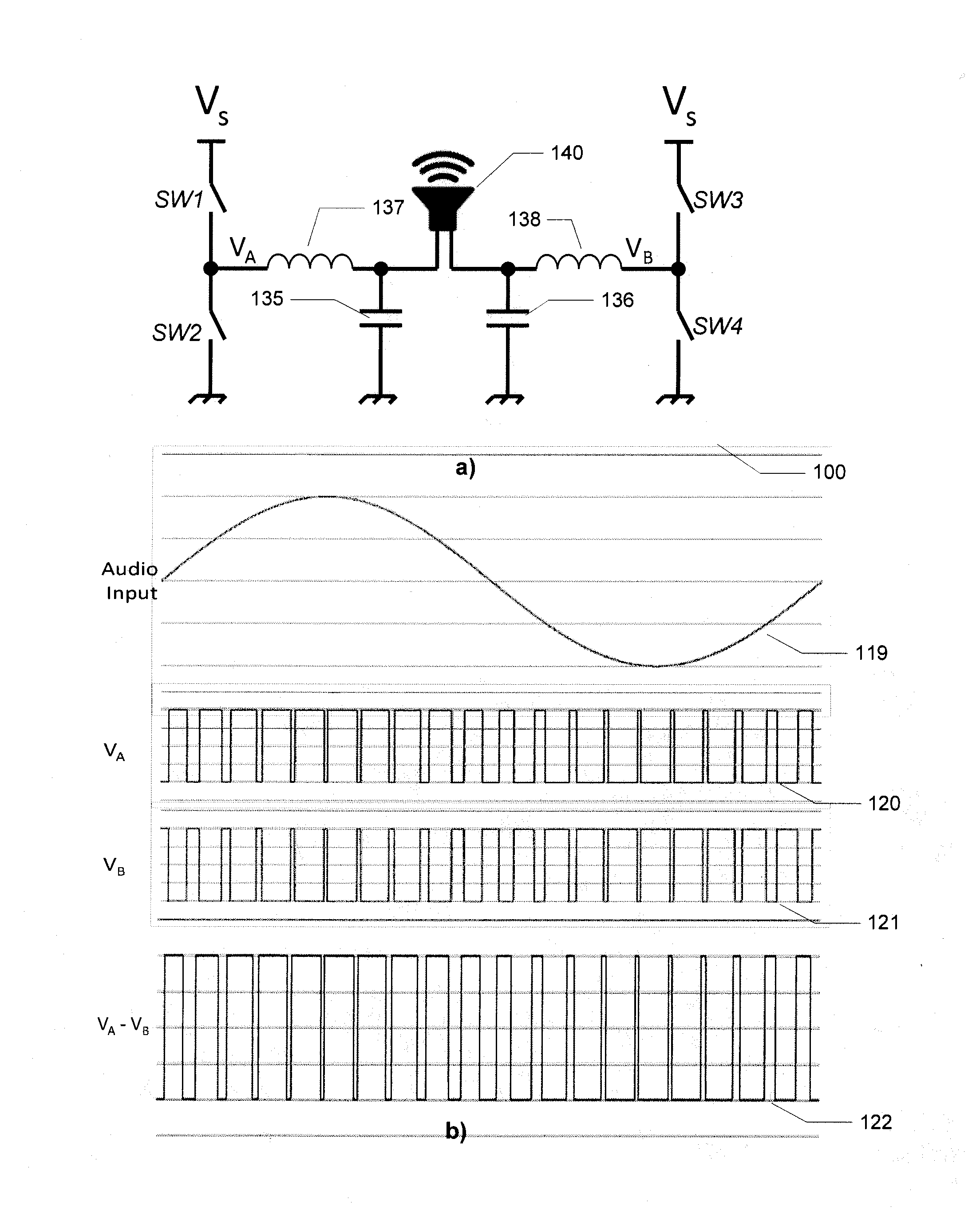
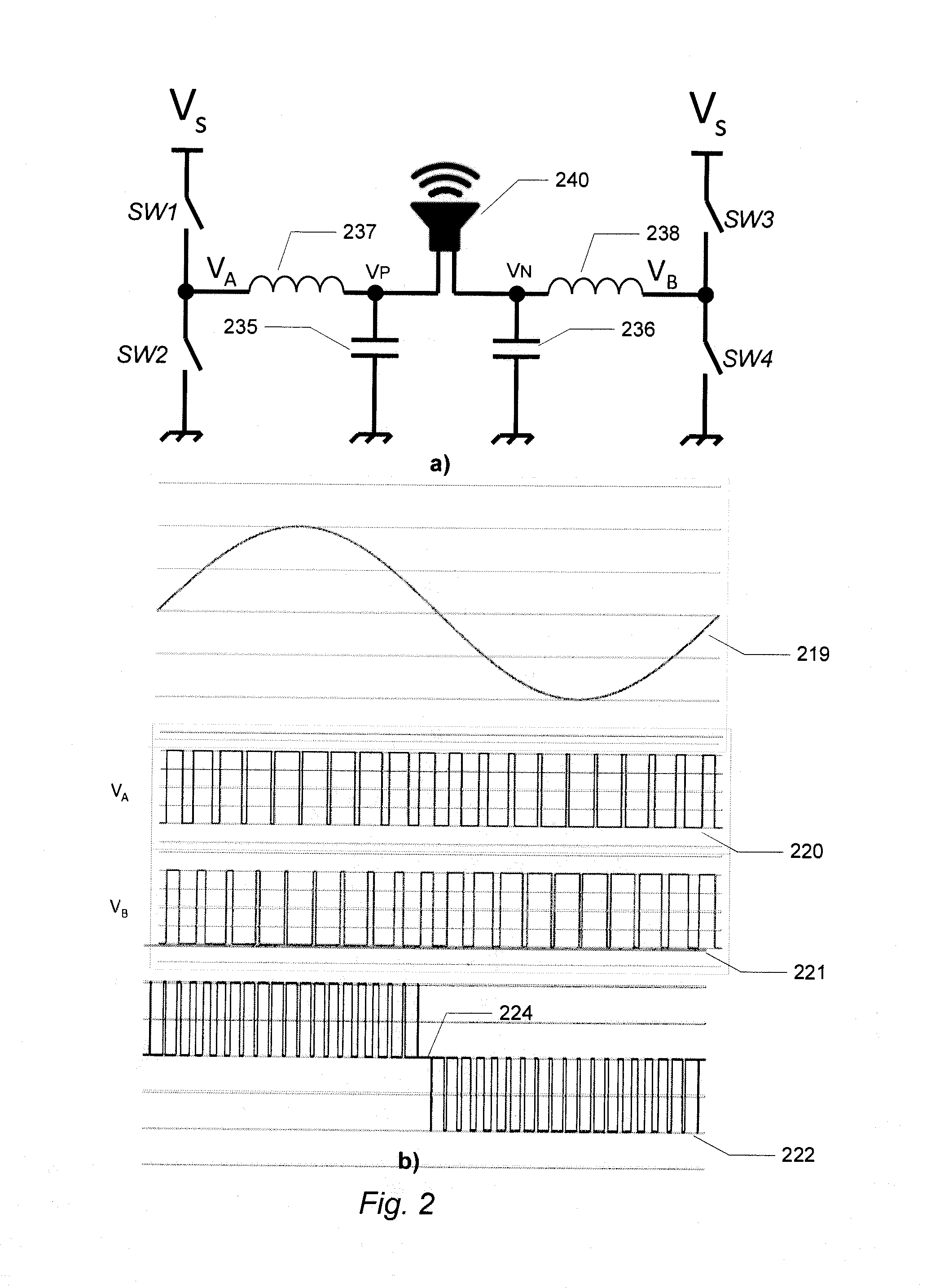
[0017]In another embodiment, the predetermined DC voltage difference differs from one half of the DC voltage difference between the first and second DC supply voltages so as to create a 4-level signal at the output node since the DC voltage source is alternatingly connected to the first DC supply voltage through the first semiconductor switch and to the second DC supply voltage through the fourth semiconductor switch. A significant advantage of the present class D audio amplifier over classic AD and BD pulse width modulation is a suppression or attenuation of common mode ripple voltage across the loudspeaker load and output filter components. This common mode ripple voltage is an unwanted residue of the switching or modulation frequency of the pulse width modulated carrier. Another other advantage is a lower output filter inductor ripple current and output filter capacitor ripple voltage at small modulation duty cycles corresponding to small levels of the audio input signal.
[0054]In one preferred embodiment, the controller is further adapted to compare the detected level of the audio input signal with a predetermined level threshold and change between the first and second operation modes depending on an outcome of the comparison. The controller compares the detected level of the audio input signal with a predetermined level threshold and selects the first operation mode when the detected audio signal level exceeds the predetermined level threshold. The controller selects the second operation mode when the detected audio signal level is smaller than the predetermined level threshold. A significant advantage of this embodiment is an acceptable level of common-mode load capacitor ripple voltage in combination with a possibility to reduce the switching frequency of the modulated control signals. The reduced switching frequency leads to an advantageous lowering of power losses in the semiconductor switches and their associated control terminal driving circuitry such as gate driver circuitry.

Problems solved by technology

The idle power consumption leads to poor power efficiency at such small audio input signals with efficiency figures far below the often quoted 90-100% power efficiency of prior art Class D amplifiers.
Operation at the quoted power efficiency is only obtained for very large audio input signals while operation within typical levels of audio input signals leads to much poorer power efficiency.
The relatively poor power efficiency at low level audio input signals are inter alia caused by the switching losses occurring in semiconductor switches of the H-bridge and a ripple currents induced in load inductors and ripple voltages induced in load capacitors.
However, load inductors and load capacitors of appropriate size for prior art class D audio amplifiers are often so large that they must be provided as external components to an integrated circuit containing other functions and circuits of the class D audio amplifier.
Consequently, the load inductors and load capacitors add to the costs of complete amplification solutions or assemblies for portable and stationary entertainment and communication equipment such as TV sets computer audio, Hi-Fi stereo amplifiers etc.
Likewise, the external inductors and capacitors require allocation of valuable board space for amplification solutions and present a potential reliability source.
Another problem associated with prior art Class D audio amplifiers is the generation of excessive levels of EMI noise by the carrier or switching frequency associated with the pulse width or density modulated audio signals that comprises essentially rectangular pulses with repetition frequencies in a range between 250 kHz-2 MHz.
The high level of EMI noise complicates integration of these prior art class D audio amplifiers with other types of signal processing circuits such as radio-frequency transmitters / receivers etc.

Method used


Image

  • Audio amplifier using multi-level pulse width modulation
  • Audio amplifier using multi-level pulse width modulation
  • Audio amplifier using multi-level pulse width modulation

Examples


first embodiment

[0114]In the invention, the various pulse width modulated control signals are configured such that the first and fifth fourth pulse width modulated control signals are in opposite phase at zero modulation. The same applies for the second and 6th pulse width modulated control signals, the third and 7th pulse width modulated control signals and the fourth and 8th pulse width modulated control signals. This configuration of the pulse width modulated control signals ensures, in combination with the respective settings of the predetermined DC voltages of the flying capacitors Cfly1 , Cfly2 (418, 419) to about one-half of the first DC supply voltage VS, that a 3-level pulse width modulated output signal is generated between the first and second output nodes VA and VB and therefore applied as a load signal to the loudspeaker load 440. This 3-level pulse width modulated output signal is illustrated on FIG. 5 as waveform 507. As illustrated the present 3-level pulse width modulated output si...

second embodiment

[0115]In the invention, the various pulse width modulated control signals are configured such that the first and fifth fourth pulse width modulated control signals are inverted and additionally phase shifted with + / −90 degrees relative to each other. The same applies for a corresponding phase relationship between the second and 6th pulse width modulated control signals, the third and 7th pulse width modulated control signals and the fourth and 8th pulse width modulated control signals. This adaptation of the pulse width modulated control signals ensures, in combination with the setting of both of the predetermined DC voltages of the flying capacitors Cfly1, Cfly2 (418, 419) to about one-half of the first DC supply voltage VS, that a 5-level pulse width modulated output signal is generated between the first and second output nodes VA and VB and therefore applied as a load signal to the loudspeaker load 440. This 5-level pulse width modulated output signal is illustrated on FIG. 5 as ...

third embodiment

[0116]FIG. 6 illustrates a CMOS based single-ended multi-level output driver 601 coupled to a loudspeaker load 640 through a lowpass filter comprising load inductor 637 and load capacitor 635 in accordance with the invention. The single-ended multi-level output driver 601 comprises, in addition to semiconductor switches SW1, SW2, SW3, SW4 of the single-ended output driver depicted on FIG. 4a), a 5th CMOS semiconductor switch SW5 and a sixth semiconductor switch SW6 to bring the total number of series coupled or connected CMOS semiconductor switches up to six. The 5th CMOS semiconductor switch SW5 is coupled in series with the upper or first DC supply voltage VS and in series to the first and second semiconductor switches SW1 and SW2 which are coupled to an output node VA. The 6th CMOS semiconductor switch SW6 is coupled in series between GND and series coupled third and fourth semiconductor switches SW3 and SW4 which are coupled to the output node VA. Consequently, both an upper leg...


PUM


Abstract

The present invention relates in one aspect to a class D audio amplifier with improved output driver topology supporting multi-level output signals such as 3-level, 4-level or 5-level pulse width or pulse density modulated output signals for application to a loudspeaker load. The present class D audio amplifiers are particularly well-suited for high-volume consumer audio applications and solutions.

Description

[0001]The present invention relates in one aspect to a class D audio amplifier with improved output driver topology supporting multi-level output signals such as 3-level, 4-level or 5-level pulse width or pulse density modulated output signals for application to a loudspeaker load. The present class D audio amplifiers are particularly well-suited for high-volume consumer audio applications and solutions.BACKGROUND OF THE INVENTION[0002]Class D audio amplifiers are a well-known type of audio power amplifier which generally is recognized to provide energy efficient audio drive of a loudspeaker load by switching a pulse width modulated (PWM) or pulse density modulated (PDM) audio signal across the loudspeaker load. Class D audio amplifiers typically comprises an H-bridge driver with a pair of output terminals coupled to respective sides or terminals of the loudspeaker load to apply an oppositely phased pulse width modulated or pulse density audio signals across the loudspeaker. Several...

Claims


Application Information

Patent Timeline
Patent Type & Authority Applications(United States)
IPC IPC(8): H03F3/00
CPCH03F3/2173H03F3/00H03F3/2178H02M7/487H02M7/4837H03F1/0244H03F3/187H03F2200/03H03F2200/267H03F2200/333H04R3/02
Inventor HOYERBY, MIKKEL
Owner INFINEON TECH AUSTRIA AG
Why Eureka
Try Eureka