Microelectronic programmable device and methods of forming and programming the same

a microelectronic and programmable technology, applied in the field of microelectronic devices, can solve the problems of increasing the voltage required to reduce the resistance of the device, and achieve the effects of reducing the cross-sectional area of the interface, increasing the efficiency of the device, and reducing the interface area

Inactive Publication Date: 2006-02-14
AXON TECH
View PDF4 Cites 58 Cited by
  • Summary
  • Abstract
  • Description
  • Claims
  • Application Information

AI Technical Summary

Benefits of technology

[0011]The ways in which the present invention addresses various drawbacks of now-known programmable devices are discussed in greater detail below. However, in general, the present invention provides a programmable device that is relatively easy and inexpensive to manufacture, and which is relatively easy to program.
[0013]In accordance with another exemplary embodiment of the invention, a programmable structure includes an ion conductor, at least two electrodes, and a barrier interposed between at least a portion of one of the electrodes and the ion conductor. In accordance with one aspect of this embodiment the barrier material includes a material configured to reduce diffusion of ions between the ion conductor and at least one electrode. The diffusion barrier may also serve to prevent undesired electrodeposit growth within a portion of the structure. In accordance with another aspect, the barrier material includes an insulating material. Inclusion of an insulating material increases the voltage required to reduce the resistance of the device. In accordance with yet another aspect of this embodiment, the barrier includes material that conducts ions, but which is relatively resistant to the conduction of electrons. Use of such material may reduce undesired plating at an electrode and increase the thermal stability of the device.
[0015]In accordance with another embodiment of the present invention, at least a portion of a programmable structure is formed within a through-hole or via in an insulating material. In accordance with one aspect of this embodiment, a first electrode feature is formed on a surface of a substrate, insulating material is deposited onto a surface of the electrode feature, a via is formed within the insulating material, and a portion of the programmable structure is formed within the via. After the via is formed within the insulating material, a portion of the structure within the via is formed by depositing an ion conductive material onto the conductive material, depositing a second electrode material onto the ion conductive material, and, if desired, removing any excess electrode, ion conductor, and / or insulating material. In accordance with another aspect of this embodiment, only the ion conductor is formed within the via. In this case, a first electrode is formed below the insulating material an in contact with the ion conductor and the second electrode is formed above the insulating material and in contact with the ion conductor. The configuration of the via may be changed to alter (e.g., reduce) a contact area between one or more of the electrodes and the ion conductor. Reducing the cross-sectional area of the interface between the ion conductor and the electrode increases the efficiency of the device (change in electrical property per amount of power supplied to the device). In accordance with another aspect of this embodiment, the via may extend through the lower electrode to reduce the interface area between the electrode and the ion conductor. In accordance with yet another aspect of this embodiment, a portion of the ion conductor may be removed from the via or the ion conductor material may be directionally deposited into only a portion of the via to further reduce an interface between an electrode and the ion conductor.

Problems solved by technology

Inclusion of an insulating material increases the voltage required to reduce the resistance of the device.

Method used


Image

  • Microelectronic programmable device and methods of forming and programming the same
  • Microelectronic programmable device and methods of forming and programming the same
  • Microelectronic programmable device and methods of forming and programming the same

Examples


Embodiment Construction

[0036]The present invention generally relates to microelectronic devices. More particularly, the invention relates to programmable structures or devices suitable for various integrated circuit applications.

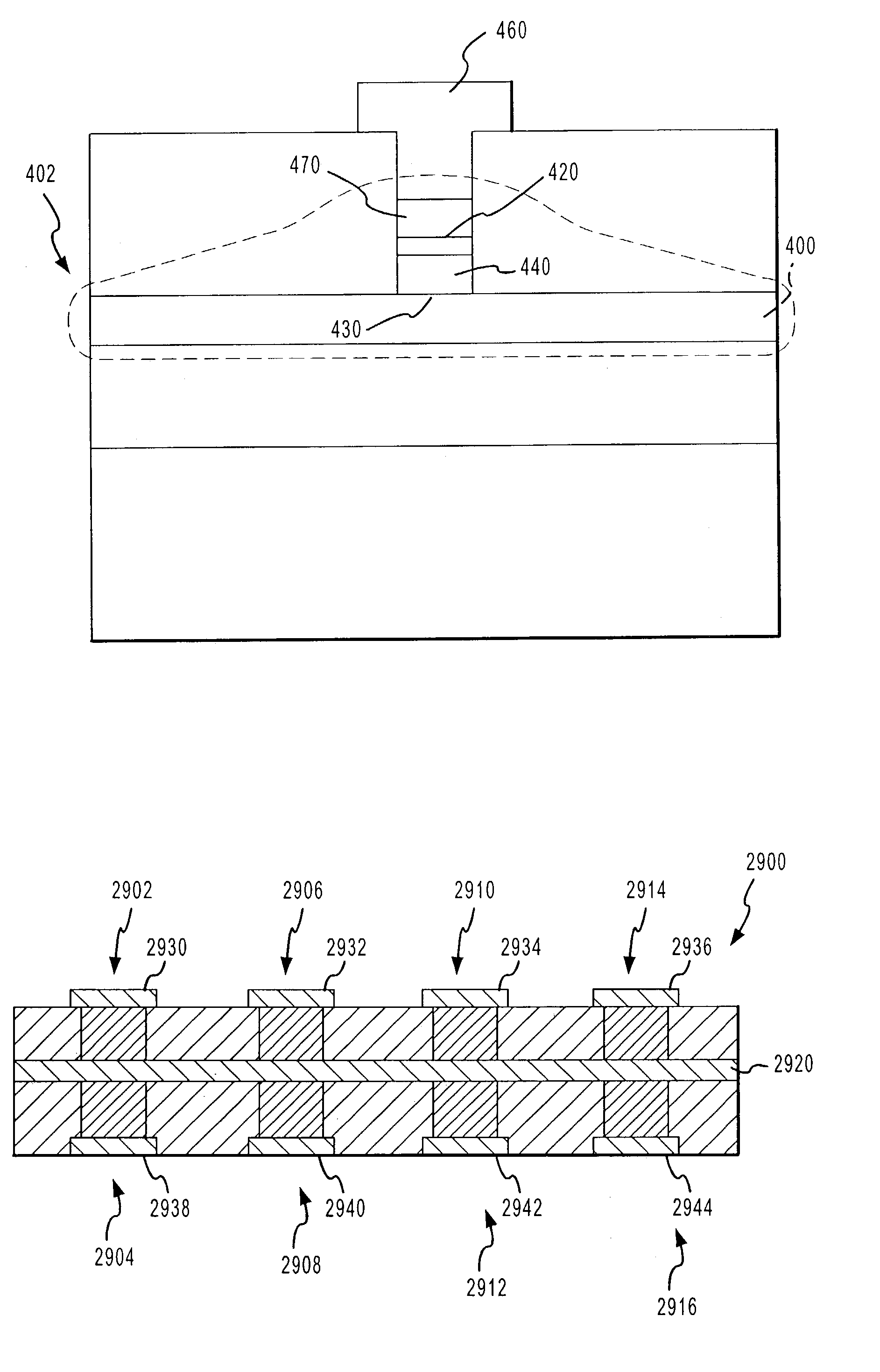
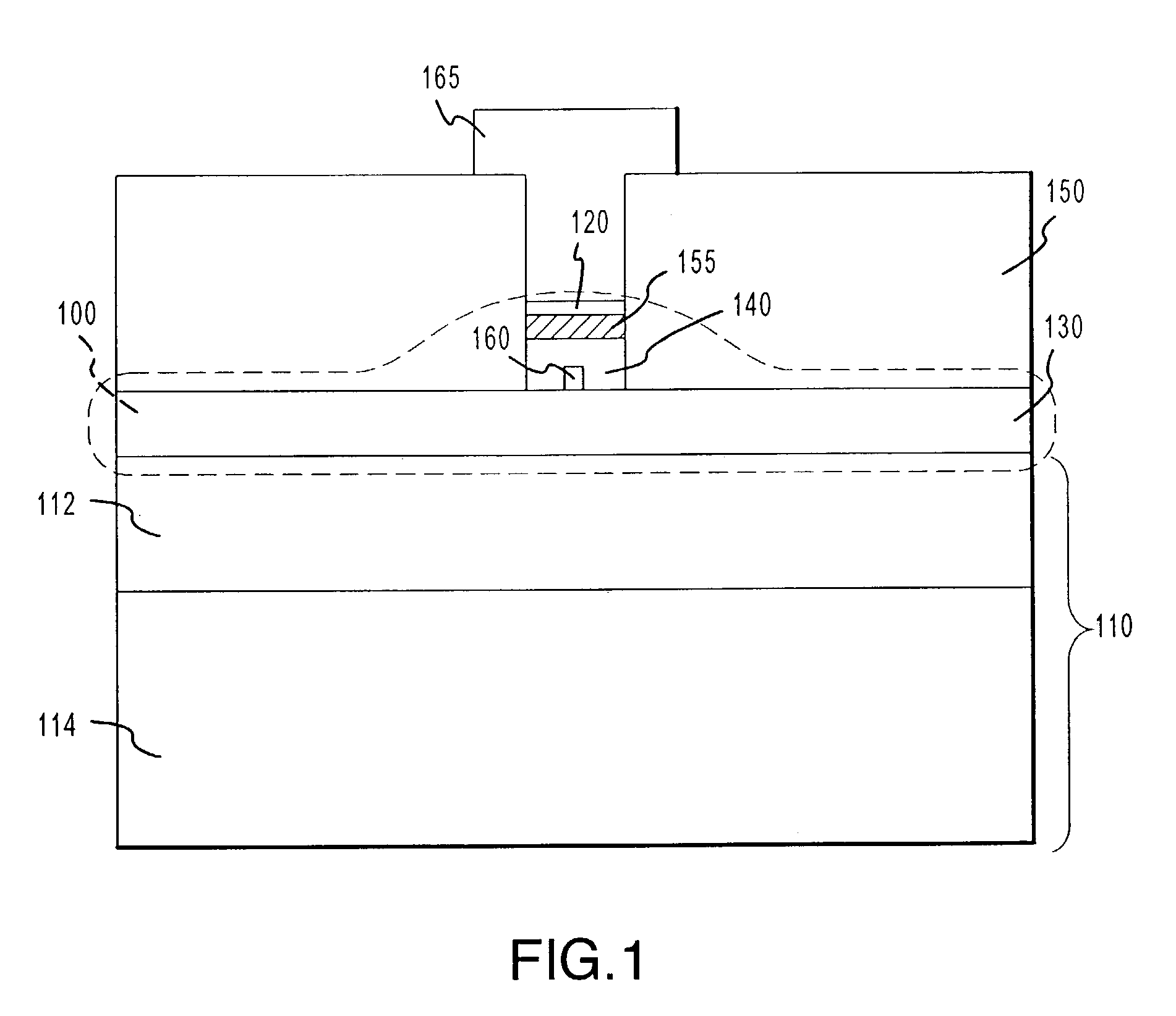
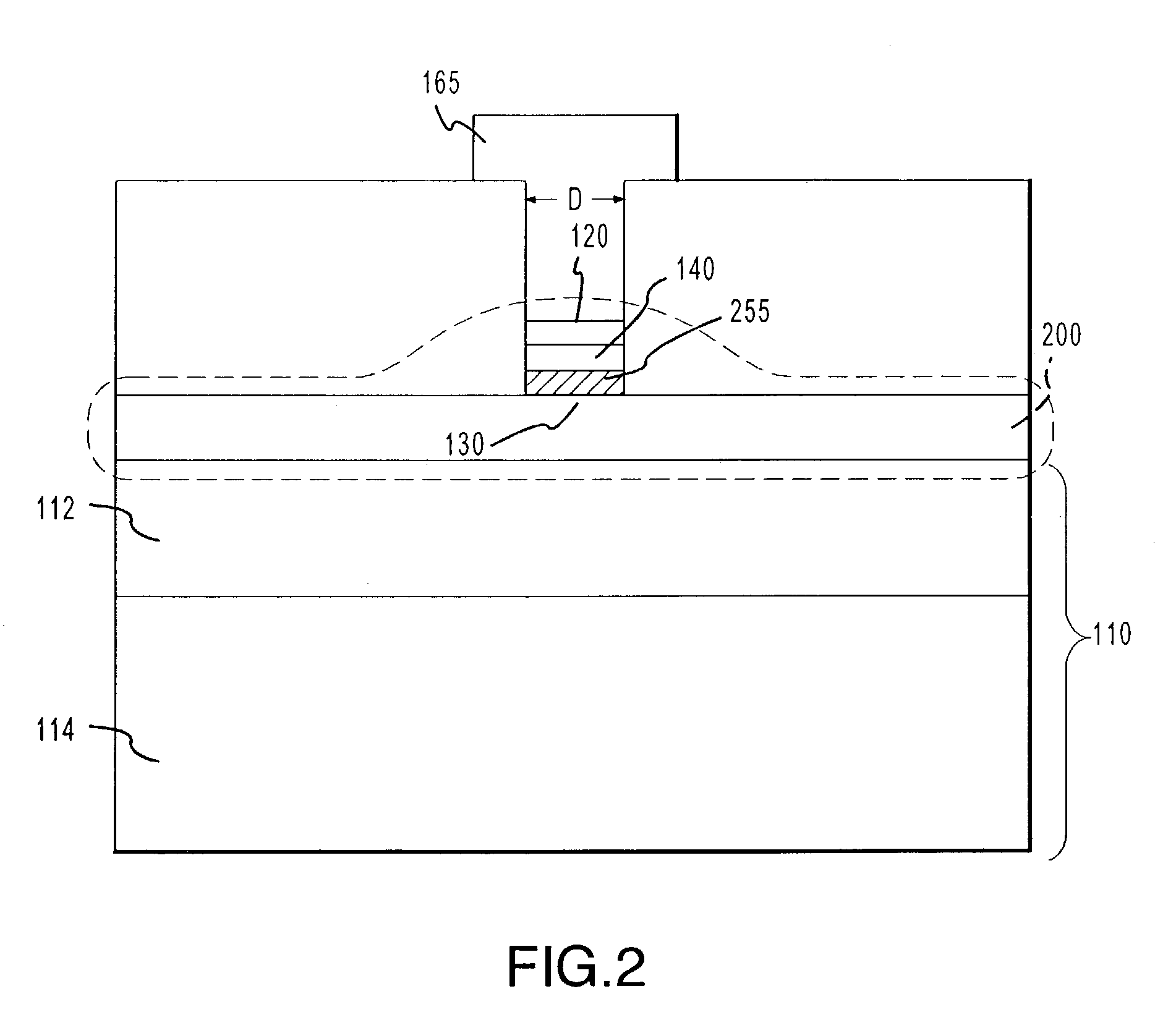
[0037]FIGS. 1 and 2 illustrate programmable microelectronic structures 100 and 200 formed on a surface of a substrate 110 in accordance with an exemplary embodiment of the present invention. Structures 100 and 200 include electrodes 120 and 130, an ion conductor 140, and optionally include buffer or barrier layers 155 and / or 255.

[0038]Generally, structures 100 and 200 are configured such that when a bias greater than a threshold voltage (VT), discussed in more detail below, is applied across electrodes 120 and 130, the electrical properties of structure 100 change. For example, in accordance with one embodiment of the invention, as a voltage V≧VT is applied across electrodes 120 and 130, conductive ions within ion conductor 140 begin to migrate and form an electrodeposit (e.g., el...


PUM


Abstract

A microelectronic programmable structure and methods of forming and programming the structure are disclosed. The programmable structure generally include an ion conductor and a plurality of electrodes. Electrical properties of the structure may be altered by applying a bias across the electrodes, and thus information may be stored using the structure.

Description

CROSS REFERENCE TO RELATED APPLICATIONS[0001]This application is a divisional of application Ser. No. 09 / 951,882, entitled MICROELECTRONIC PROGRAMMABLE DEVICE AND METHODS OF FORMING AND PROGRAMMING THE SAME, filed Sep. 10, 2001, now U.S. Pat. No. 6,635,914, which is a Continuation in Part of U.S. patent application Ser. No. 09 / 502,915, entitled PROGRAMMABLE MICROELECTRONIC DEVICES AND METHODS OF FORMING AND PROGRAMMING SAME, filed Feb. 11, 2000, now U.S. Pat. No. 6,487,106, which is a Continuation in Part of U.S. patent application Ser. No. 09 / 555,612, entitled PROGRAMMABLE SUBSURFACE AGGREGATING METALLIZATION CELL STRUCTURE AND METHOD OF MAKING SAME, filed Dec. 4, 1998, now U.S. Pat. No. 6,418,049; and which claims the benefit of; U.S. patent application Ser. No. 60 / 231,343, entitled COMMON ELECTRODE CONFIGURATIONS OF THE PROGRAMMABLE METALLIZATION CELL, filed Sep. 8, 2000; U.S. patent application Ser. No. 60 / 231,345, entitled GLASS COMPOSITION SUITABLE FOR PROGRAMMABLE METALLIZATI...

Claims


Application Information

Patent Timeline
Patent Type & Authority Patents(United States)
IPC IPC(8): H01L21/336G06K15/10G11C11/00G11C11/56G11C13/02H01L27/10H01L27/24H01L31/0336H01L45/00H04N1/405H04N1/52
CPCG06K15/107H01L45/1658G11C11/00G11C11/5614G11C13/0011H01L27/101H01L27/2481H01L45/085H01L45/1226H01L45/1233H01L45/1253H01L45/1266H01L45/142H01L45/143H01L45/1616H01L45/1625H01L45/1675H01L45/1683H04N1/4051H04N1/52H01L45/124H01L45/1691H01L27/2463G11C13/04G11C2207/104G11C2213/15G11C2213/51G11C2213/55G11C2213/72G11C2213/79H01L27/2409H01L27/2436Y10S438/933G06K2215/0094H10B63/84H10B63/20H10B63/30H10B63/80H10N70/245H10N70/8265H10N70/823H10N70/841H10N70/8416H10N70/8822H10N70/8825H10N70/826H10N70/026H10N70/023H10N70/046H10N70/068H10N70/066H10N70/063
Inventor KOZICKI, MICHAEL N.MITKOVA, MARIA
Owner AXON TECH
Why Eureka
Try Eureka