Programming circuit for a programmable microelectronic device, system including the circuit, and method of forming the same

a microelectronic device and programming circuit technology, applied in the field of programming circuits, can solve the problems of high cost of manufacture, large energy consumption for data storage, and particularly volatile dynamic ram (“dram”), and achieve the effect of easy and inexpensive manufacture and easy programing

Inactive Publication Date: 2005-03-08
AXON TECH
View PDF1 Cites 75 Cited by
  • Summary
  • Abstract
  • Description
  • Claims
  • Application Information

AI Technical Summary

Benefits of technology

The ways in which the present invention addresses various drawbacks of now-known programmable devices and systems are discussed in greater detail below. However, in general, the present invention provides a programming circuit and a corresponding programmable device that are relatively easy and inexpensive to manufacture and are relatively easy to program.

Problems solved by technology

Dynamic RAM (“DRAM”) is particularly volatile in that it must be “refreshed” (i.e., recharged) every few hundred milliseconds in order to maintain the stored data.
Static RAM (“SRAM”) will hold the data after one writing so long as the power source is maintained; once the power source is disconnected, however, the data is lost.
In general, these RAM devices can take up significant chip area and therefore may be expensive to manufacture and consume relatively large amounts of energy for data storage.
Other storage devices such as magnetic storage devices (e.g., floppy disks, hard disks and magnetic tape) as well as other systems, such as optical disks, CD-RW and DVD-RW are non-volatile, have extremely high capacity, and can be rewritten many times. Unfortunately, these memory devices are physically large, are shock / vibration-sensitive, require expensive mechanical drives, and may consume relatively large amounts of power.
These negative aspects make such memory devices non-ideal for low power portable applications such as lap-top and palm-top computers, personal digital assistants (“PDAs”), and the like.
Furthermore, because these portable systems often require data storage when the power is turned off, nor-volatile storage device are desired for use in such systems.
Once programmed, the WORM device cannot be reprogrammed.
Thus, such devices are generally not well suited for use in portable electronic devices.
EEPROM devices are generally easier to program, but suffer from other deficiencies.
In particular, EEPROM devices are relatively complex, are relatively difficult to manufacture, and are relatively large.
Consequently, EEPROM cost per bit of memory capacity is extremely high compared with other means of data storage.
Another disadvantage of EEPROM devices is that, although they can retain data without having the power source connected, they require relatively large amounts of power to program.
This power drain can be considerable in a compact portable system powered by a battery.
Other forms of electronic memory such as FLASH memory are also relatively expensive and complicated to manufacture.

Method used


Image

  • Programming circuit for a programmable microelectronic device, system including the circuit, and method of forming the same
  • Programming circuit for a programmable microelectronic device, system including the circuit, and method of forming the same
  • Programming circuit for a programmable microelectronic device, system including the circuit, and method of forming the same

Examples


Embodiment Construction

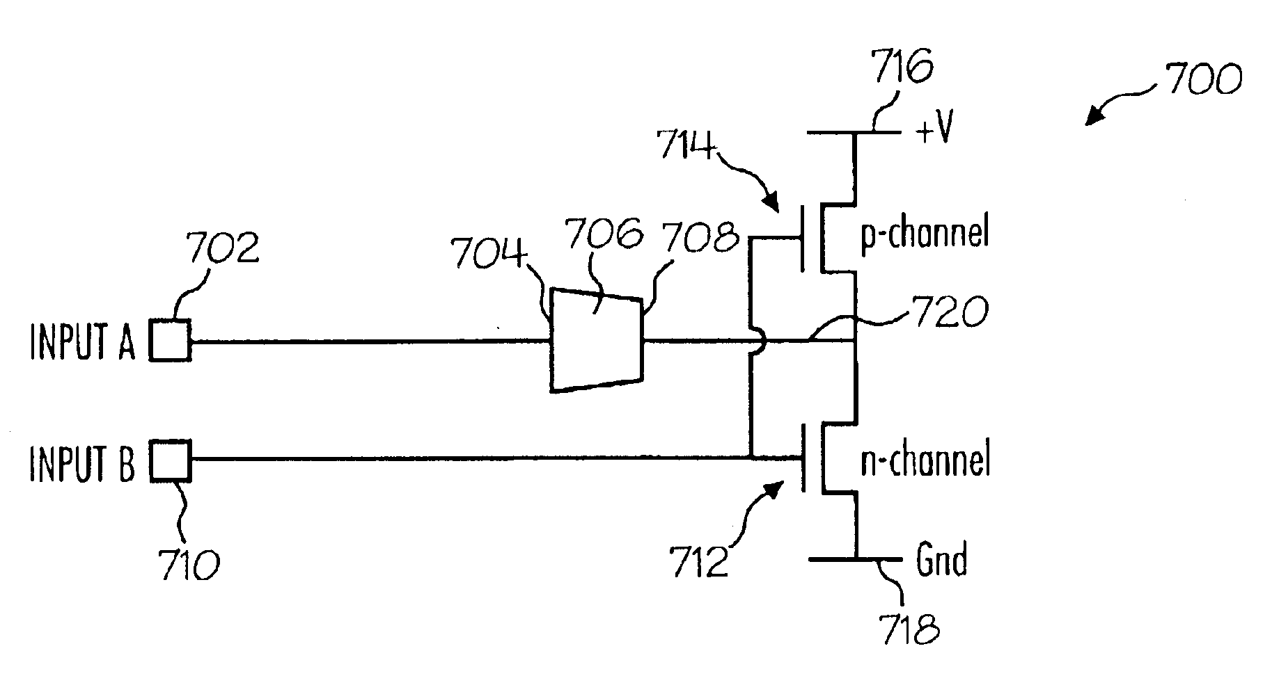
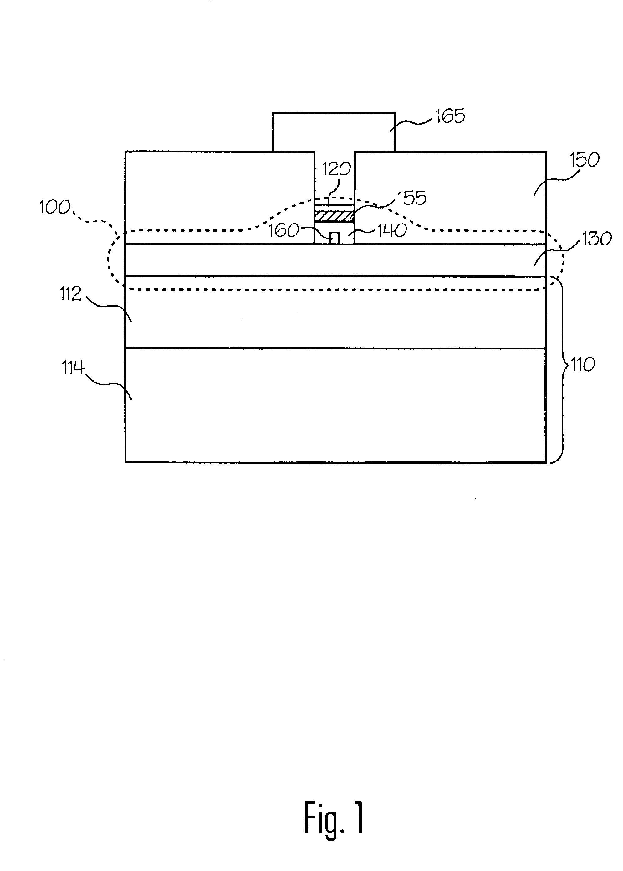
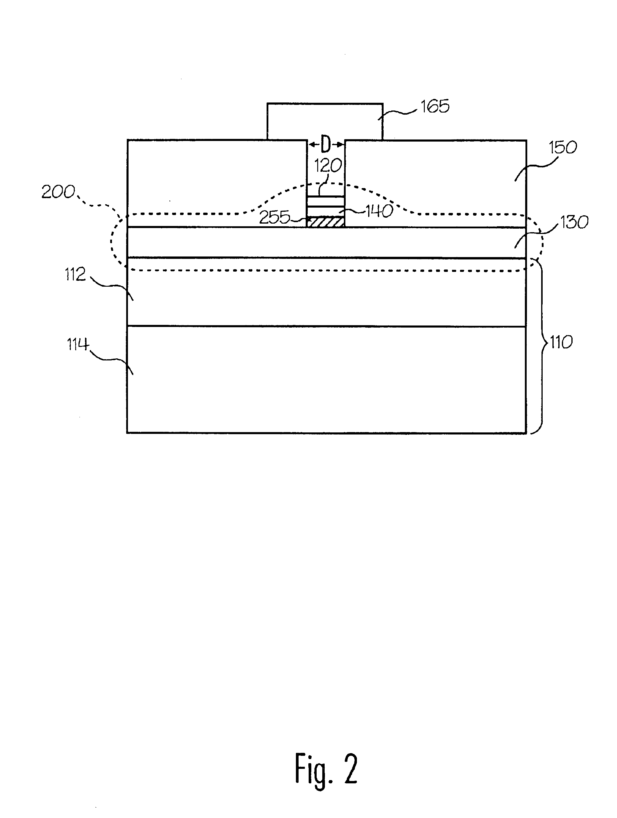
The present invention may be described herein in terms of various functional components. It should be appreciated that such functional components may be realized by any number of hardware or structural components configured to perform the specified functions. For example, the present invention may employ various integrated components comprised of various electrical devices, e.g., resistors, transistors, capacitors, diodes and the like, whose values may be suitably configured for various intended purposes. In addition, the present invention may be practiced in any integrated circuit application where an effective reversible polarity is desired. Such general applications that may be appreciated by those skilled in the art in light of the present disclosure are not described in detail. Further, it should be noted that while various components may be suitably coupled or connected to other components within exemplary circuits, such connections and couplings can be realized by direct conn...


PUM


Abstract

A circuit for programming a microelectronic device is disclosed. The circuit is configured to provide a reversible bias across the microelectronic device to perform erase and write functions. One configuration of the programming circuit includes one or more inputs coupled to the programmable device and a complimentary metal-oxide semiconductor circuit coupled to the programmable device. This design allows for writing and erasing of the programmable cell using a low and high voltage input.

Description

1. Field of InventionThe present invention generally relates to programmable microelectronic devices. More particularly, the invention relates to a circuit for applying a write and / or erase voltage to a device having an electrical property that can be variably programmed by manipulating an amount and / or polarity of energy supplied to the device.2. Background of the InventionMemory devices are often used in electronic systems and computers to store information in the form of binary data. These memory devices may be characterized into various types, each type having associated with it various advantages and disadvantages.For example, random access memory (“RAM”), which may be found in personal computers, is typically volatile semiconductor memory; in other words, the stored data is lost if the power source is disconnected or removed. Dynamic RAM (“DRAM”) is particularly volatile in that it must be “refreshed” (i.e., recharged) every few hundred milliseconds in order to maintain the st...

Claims


Application Information

Patent Timeline
Patent Type & Authority Patents(United States)
IPC IPC(8): G11C11/56G11C16/02G11C13/02G11C11/34H01L27/24H01L27/10
CPCB82Y10/00G11C11/5614G11C13/0011G11C13/0069H01L27/101G11C2207/104G11C2213/51G11C2213/72G11C2213/79G11C2013/009
Inventor KOZICKI, MICHAEL N.
Owner AXON TECH
Why Eureka
Try Eureka