Light-receiving panel or light-emitting panel, and manufacturing method thereof

Inactive Publication Date: 2006-03-02
SPHELAR POWER
View PDF30 Cites 76 Cited by
  • Summary
  • Abstract
  • Description
  • Claims
  • Application Information

AI Technical Summary

Benefits of technology

[0013] In this light receiving or light emitting panel, since numerous semiconductor elements are incorporated on one printed wiring sheet, with intermediate parts in the direction of height of the respective semiconductor elements being held by the retaining holes, and since the pairs of electrodes of the respective semiconductor elements are connected to the printed wiring, the installation, positioning and electrical connection of the numerous semiconductor elements can easily be accomplished. Since a single printed wiring sheet is incorporated in substantially an intermediate position in the direction of thickness of the light receiving or light emitting panel, the thickness of the light receiving or light emitting panel can

Problems solved by technology

In this case, however, since numerous electrodes must be connected with a plurality of solar cells precisely positioned on a printed board, and numerous electrodes must be connected with another printed board superimposed on top of this assembly, the structure of the solar cell panel becomes complicated; furthermore, the size of the panel is increased, and the cost of parts and cost of assembly are increased, so that the manufacturing cost of the solar cell panel is increased.
In the case of this solar cell panel, the manufacture of the mesh having a special structure is not easy, and the manufacturing cost is also high; however, a solar cell pa

Method used


Image

  • Light-receiving panel or light-emitting panel, and manufacturing method thereof
  • Light-receiving panel or light-emitting panel, and manufacturing method thereof
  • Light-receiving panel or light-emitting panel, and manufacturing method thereof

Examples


Example

[0060] Embodiments of the present invention will be described below with reference to the attached drawings.

[0061] The present embodiment is an example of a case in which the present invention is applied to a solar cell panel as a light receiving panel. A method for manufacturing this solar cell panel, and the structure of this solar cell panel, will be described.

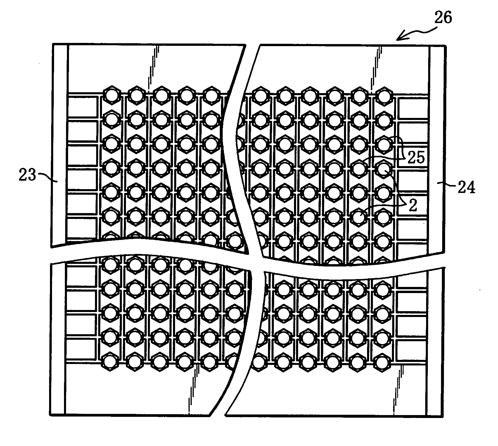
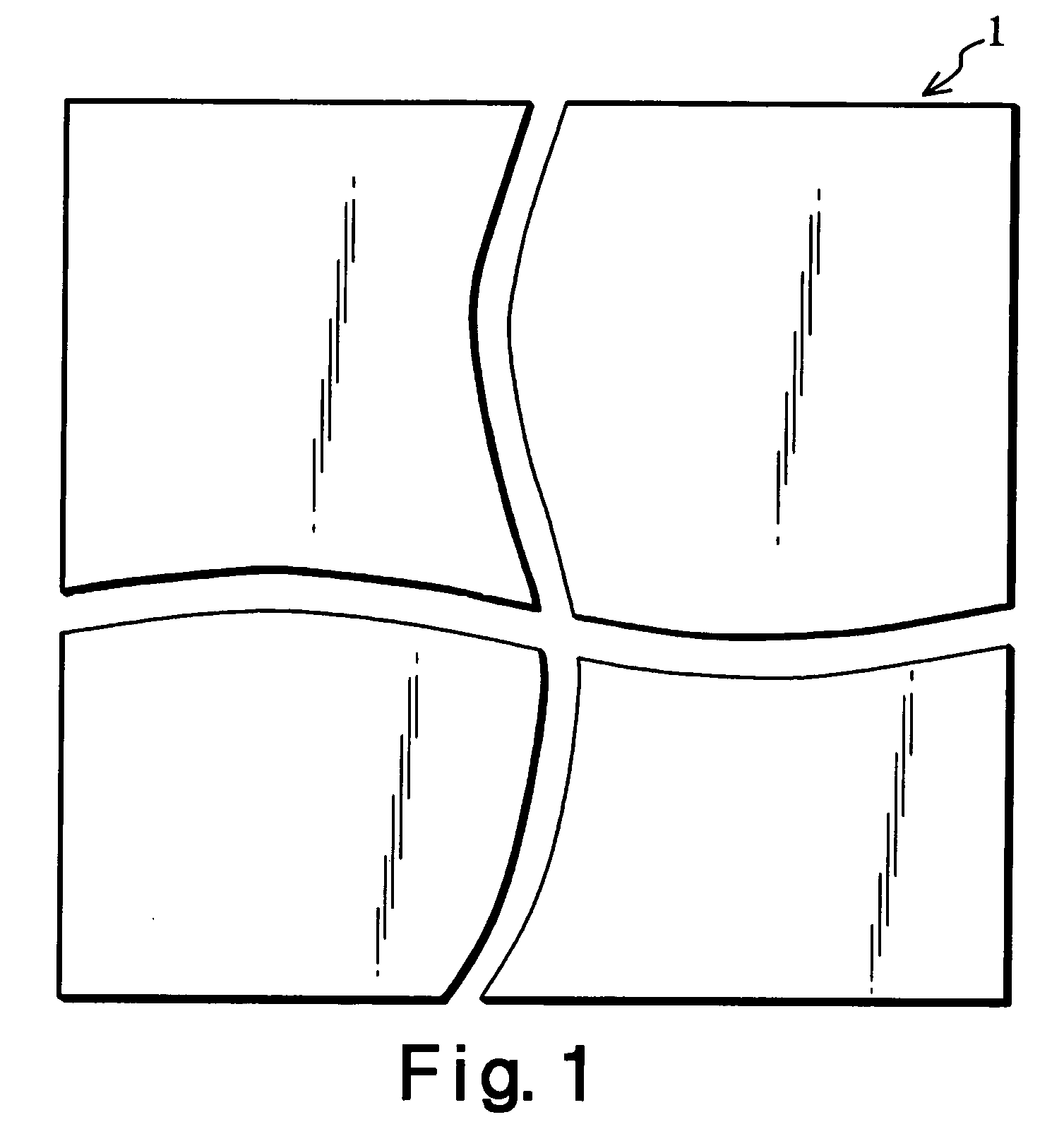
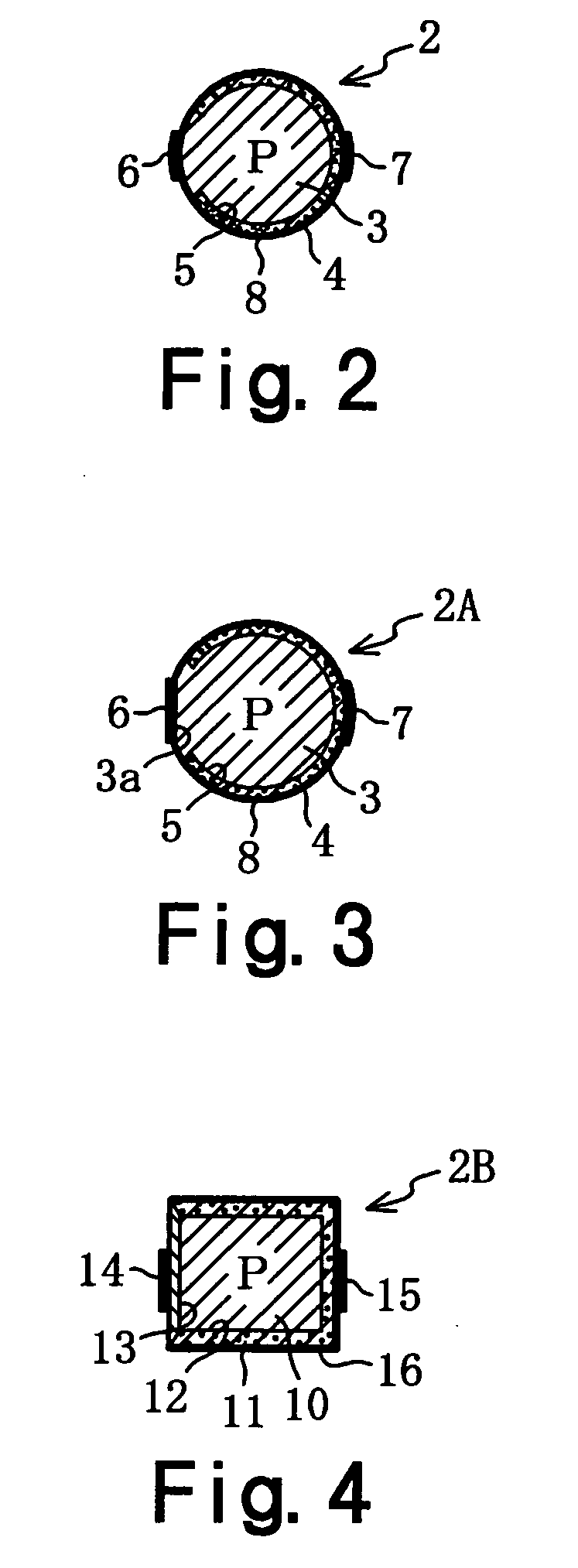
[0062] First, in a first step, the printed wiring sheet material 1 shown in FIG. 1, and numerous particulate semiconductor elements 2 (3600 elements in the present embodiment, hereafter referred to as “solar cells”) that have a light-to-electricity transducing function, are prepared.

[0063] As is shown in FIG. 1, the printed wiring sheet material 1 is a flat-plate material that is formed by cutting a thin transparent sheet material such as an epoxy type synthetic resin, acrylic type synthetic resin, polyester type synthetic resin, polycarbonate or the like (for example thickness 0.4 to 0.6 mm, 0.6 mm in the present embodi...


PUM


Abstract

A light receiving panel provided with a plurality of particulate semiconductor elements (solar cells) or a light emitting panel provided with a plurality of particulate semiconductor elements (light emitting diodes) is disclosed. In the solar cell panel, a printed wiring sheet is constructed by forming printed wiring and retaining holes in the form of a matrix with a plurality of rows and a plurality of columns in a printed wiring sheet material made of a thin transparent synthetic resin; a plurality of solar cells are respectively mounted in the plurality of retaining holes, these cells are resin-sealed by a transparent synthetic resin material, a positive pole terminal and negative pole terminal exposed to the outside are formed, and a plurality of solar cell panels are constructed so that series connection, parallel connection or series-parallel connection is possible. The solar cell panel may also be constructed so that deformation in the manner of two dimensional or three dimensional curved surface is possible.

Description

TECHNICAL FIELD [0001] The present invention relates to a light receiving or light emitting panel which can be simply manufactured by mounting light receiving elements or light emitting elements in a plurality of retaining holes formed in a printed wiring sheet, and then sealing these mounted elements with a resin, and a method of manufacturing such a panel. BACKGROUND OF THE INVENTION [0002] In a conventional solar cell, an n type diffusion layer is formed on the surface of a p type semiconductor substrate, a light receiving surface electrode with a herringbone pattern is formed on the front surface side, a back surface electrode is formed on the back surface side, and the overall device is constructed as a flat-plate panel structure. In such a flat-plate solar cell panel, when the angle of incidence of sunlight increases in the morning and evening, the proportion of reflected light increases, and the proportion of light that enters the panel drops. [0003] Conventionally, therefore...

Claims


Application Information

Patent Timeline
IPC IPC(8): H01L31/12H01L31/042H01L25/075H01L31/0352H01L33/00H01L33/30H01L33/58
CPCH01L25/0753H01L25/0756H01L31/035281H01L31/048H01L33/20H01L31/0508Y02E10/50H01L2924/1017H01L2924/0002H01L33/24H01L2924/00
Inventor NAKATA
Owner SPHELAR POWER
Why Eureka
Try Eureka