Display panel and electronic device

a technology of electronic devices and display panels, applied in the field of display technology, can solve the problems of large space requirements, difficult to achieve narrow border regions, and bulky display panels

Active Publication Date: 2019-03-05
WUHAN TIANMA MICRO ELECTRONICS CO LTD +1
View PDF31 Cites 2 Cited by
  • Summary
  • Abstract
  • Description
  • Claims
  • Application Information

AI Technical Summary

Benefits of technology

[0007]Another aspect of the present disclosure provides an electronic device. The electronic device comprises a display panel. The display panel comprises a base substrate including a display region and a border region surrounding the display region, wherein the border region includes an encapsulation region; a plurality of display units disposed in the display region; an encapsulation member disposed in the border region; a plurality of wires disposed in the border region; and a cover substrate arranged opposite to the base substrate. The display units and the wires are disposed between the base substrate and the cover substrate, the encapsulation member is disposed in the encapsulation region and configured to bond and fix the base substrate to the cover substrate, and at least one of the wires is disposed in the encapsulation region.

Problems solved by technology

To efficiently prevent moisture and oxygen from penetrating the display panel, the border region of the current display panel may be substantially wide, i.e., a narrow border region may be difficult to be achieved.
Thus, the display panel may be bulky, and may require a large space to fit inside the electronic device.

Method used


Image

  • Display panel and electronic device
  • Display panel and electronic device
  • Display panel and electronic device

Examples


Embodiment Construction

[0019]Reference will now be made in detail to exemplary embodiments of the invention, which are illustrated in the accompanying drawings. Hereinafter, embodiments consistent with the disclosure will be described with reference to drawings. Wherever possible, the same reference numbers will be used throughout the drawings to refer to the same or like parts. It is apparent that the described embodiments are some but not all of the embodiments of the present invention. Based on the disclosed embodiments, persons of ordinary skill in the art may derive other embodiments consistent with the present disclosure, all of which are within the scope of the present invention. Further, in the present disclosure, the disclosed embodiments and the features of the disclosed embodiments may be combined under conditions without conflicts.

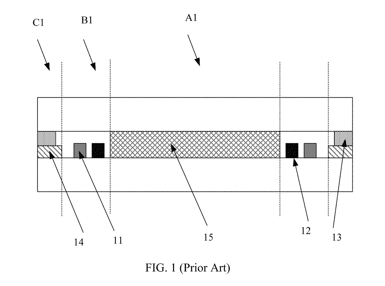
[0020]FIG. 1 illustrates a cross-sectional view of a current display panel. As shown in FIG. 1, the current display panel includes a display region A1 and a border r...


PUM

PropertyMeasurementUnit
widthaaaaaaaaaa
widthaaaaaaaaaa
widthaaaaaaaaaa

Abstract

A display panel and an electronic device are provided. The display panel comprises a base substrate including a display region and a border region surrounding the display region, wherein the border region includes an encapsulation region; a plurality of display units disposed in the display region; an encapsulation member disposed in the border region; a plurality of wires disposed in the border region; and a cover substrate arranged opposite to the base substrate. The display units and the wires are disposed between the base substrate and the cover substrate, the encapsulation member is disposed in the encapsulation region and configured to bond and fix the base substrate to the cover substrate, and at least one of the wires is disposed in the encapsulation region.

Description

CROSS-REFERENCES TO RELATED APPLICATIONS[0001]This application claims priority of Chinese Patent Application No. 201610279045.6, filed on Apr. 29, 2016, the entire contents of which are hereby incorporated by reference.FIELD OF THE INVENTION[0002]The present disclosure generally relates to the field of display technology and, more particularly, relates to a display panel and an electronic device thereof.BACKGROUND[0003]With the continuous development of science and technology, more and more electronic devices with display functions are used in people's daily life and work, which currently have brought great convenience to and become indispensable tools to ordinary people. Display panel is an essential component for the electronic device to achieve the display function. A display panel often has a display region and a border (or a frame) region. The display region is disposed with pixel units for displaying images, and the border region is disposed with scanning lines and signal line...

Claims


Application Information

Patent Timeline
Patent Type & Authority Patents(United States)
IPC IPC(8): G02F1/1362H01L27/32H01L51/00G06F1/16G02F1/1339H01L51/52G02F1/1368G02F1/1333
CPCH01L27/3276G02F1/1339G02F1/136286G06F1/163G06F1/1637H01L51/0096H01L51/5246H01L51/5243G02F2201/56G02F1/1368G02F2001/133311G02F2001/136295G02F2202/28H01L2251/53G02F1/1333G02F1/1345H10K59/00G02F2201/12G02F2201/50G02F2201/501Y02E10/549H10K50/8426G02F1/133311G02F1/136295H10K59/131H10K50/8423H10K77/10H10K2102/302
Inventor LI, CHUNYANGQIAN, DONG
Owner WUHAN TIANMA MICRO ELECTRONICS CO LTD
Why Eureka
Try Eureka