Display device and optical compensation method of a display device

a display device and optical compensation technology, applied in the field of display devices, can solve the problems of inability or inability of the optical compensation method to adequately compensate the grayscale, uneven characteristics of thin film transistors, uneven current-voltage characteristics, etc., to achieve the effect of improving the optical compensation process, and improving the quality of display images

Active Publication Date: 2019-04-02
SAMSUNG DISPLAY CO LTD
View PDF8 Cites 3 Cited by
  • Summary
  • Abstract
  • Description
  • Claims
  • Application Information

AI Technical Summary

Benefits of technology

[0007]Some example embodiments provide an emission driver that can finely control a light emission time of pixels.
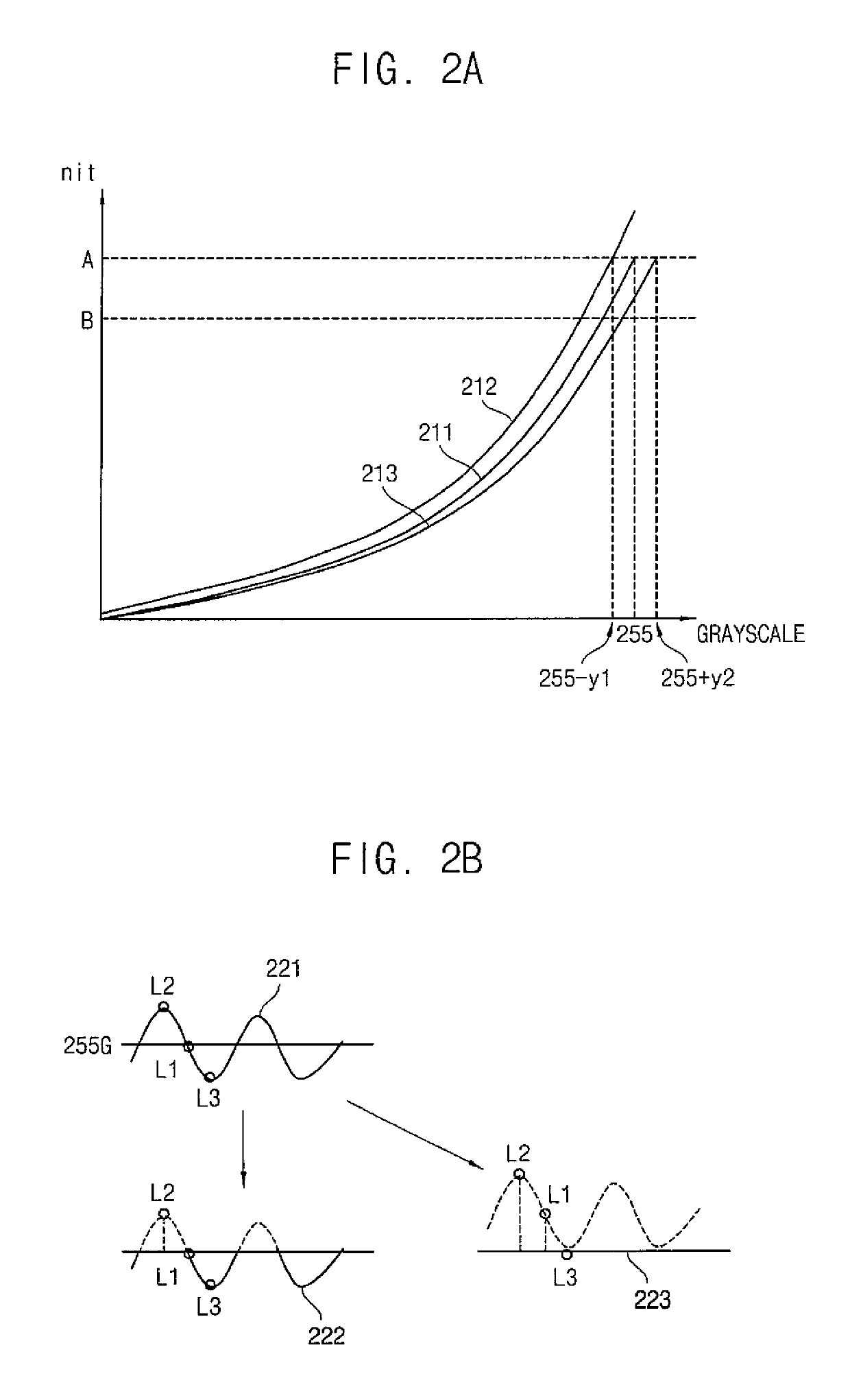
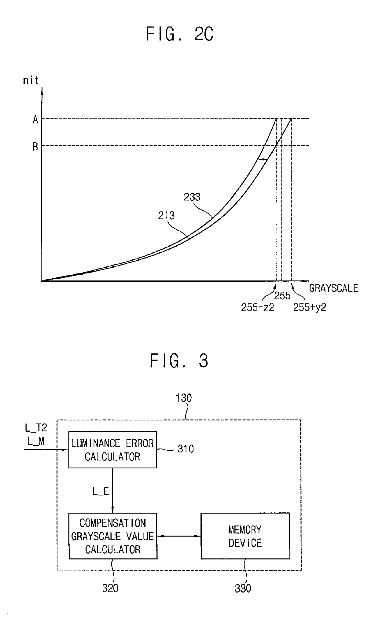
[0029]An optical compensation method of a display device according to example embodiments may eliminate or substantially eliminate (e.g., remove or prevent) a stain phenomenon of a display panel by calculating a compensation grayscale value based on a grayscale value (e.g., a maximum grayscale value) and a second target luminance that is lower than a first target luminance based on the grayscale value, and by performing a multi-time program (e.g., a post-MTP) based on the grayscale value and the first target luminance.
[0030]In addition, an optical compensation method of a display device according to example embodiments may provide a simplified optical compensation process by performing a multi-time program (e.g., a pre-MTP) based on the grayscale value (e.g., the maximum grayscale value) and a third target luminance that is higher than a first target luminance based on the grayscale value, and by calculating a compensation grayscale value based on the grayscale value and the first target luminance.
[0031]Furthermore, a display device according to example embodiments may have improved display quality (e.g., a quality of a displayed image may be improved) by using a compensation grayscale value that is generated by the optical compensation method.

Problems solved by technology

However, thin film transistors may have uneven characteristics (e.g., uneven current-voltage characteristics) due to the crystallization process.
The optical compensation method can compensate a grayscale value when the pixel emits light having a relatively high luminance; however, the optical compensation method cannot or cannot adequately compensate a grayscale value when the pixel emits light having a relatively low luminance because the optical compensation method cannot increase the grayscale value over a maximum grayscale value.

Method used


Image

  • Display device and optical compensation method of a display device
  • Display device and optical compensation method of a display device
  • Display device and optical compensation method of a display device

Examples


Embodiment Construction

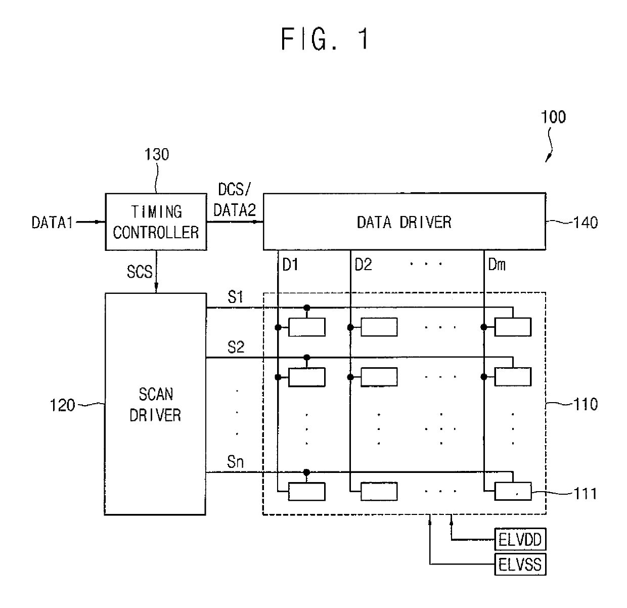
[0044]Hereinafter, aspects of the present inventive concept will be explained in detail with reference to the accompanying drawings.

[0045]It will be understood that when an element or layer is referred to as being “on,”“connected to,” or “coupled to” another element or layer, it may be directly on, connected, or coupled to the other element or layer or one or more intervening elements or layers may also be present. When an element is referred to as being “directly on,”“directly connected to,” or “directly coupled to” another element or layer, there are no intervening elements or layers present. For example, when a first element is described as being “coupled” or “connected” to a second element, the first element may be directly coupled or connected to the second element or the first element may be indirectly coupled or connected to the second element via one or more intervening elements. The same reference numerals designate the same elements. As used herein, the term “and / or” inclu...


PUM


Abstract

An optical compensation method for a display device including a pixel is provided. The method includes: providing test data having a first grayscale value to the display device; measuring a luminance of the pixel which emits light based on the test data; and calculating a compensation grayscale value based on a second target luminance and the measured luminance of the pixel. The second target luminance is lower than a first target luminance which is set based on the first grayscale value.

Description

CROSS-REFERENCE TO RELATED APPLICATION[0001]This application claims priority under 35 U.S.C. § 119 to and the benefit of Korean Patent Application No. 10-2016-0006311, filed on Jan. 19, 2016 in the Korean Intellectual Property Office (KIPO), the contents of which are incorporated herein in their entirety by reference.BACKGROUND[0002]1. Field[0003]Example embodiments relate to a display device.[0004]2. Description of the Related Art[0005]An organic light emitting display device includes pixels, and each of the pixels includes an organic light emitting diode and a thin film transistor which drives the organic light emitting diode. The thin film transistor may be formed through a crystallization process (e.g., a melting process and a solidification process) of a low-temperature poly-silicon (LTPS). However, thin film transistors may have uneven characteristics (e.g., uneven current-voltage characteristics) due to the crystallization process.[0006]An optical compensation method is propo...

Claims


Application Information

Patent Timeline
Patent Type & Authority Patents(United States)
IPC IPC(8): G09G3/20G09G3/3208
CPCG09G3/2092G09G3/3208G09G2310/08G09G2320/029G09G2320/0693G09G2320/0276G09G2320/0646G09G2320/0673G09G2320/0233G09G3/3225G09G2320/0626
Inventor CHA, UI-YEONGKIM, DAN-BIKIM, IN-HWANJUN, BYUNG-GEUN
Owner SAMSUNG DISPLAY CO LTD
Why Eureka
Try Eureka