Method for manufacturing semiconductor device

a semiconductor and manufacturing technology, applied in the field of semiconductor devices manufacturing, can solve the problems of accuracy and resolution of alignment marks affecting alignment errors, and achieve the effect of improving optical resolution and image contras

Active Publication Date: 2019-04-30
UNITED MICROELECTRONICS CORP +1
View PDF10 Cites 0 Cited by
  • Summary
  • Abstract
  • Description
  • Claims
  • Application Information

AI Technical Summary

Benefits of technology

[0004]It is therefore an objective of the present invention to provide a method for manufacturing a semiconductor device to increase the resolution of the alignment mark.
[0006]In the method of manufacturing the semiconductor device of the present invention, the mask material layer in the second gaps and the third gap are removed, and the second mask pattern which top surface is lower than the top surface of the first mask pattern remains in the first gap when the mask material layer in the peripheral region is fully removed, such that the following pattern transferring process may form the fourth trench which depth is deeper than the depth of the third trench in the semiconductor substrate in the cutting line region. Accordingly, an image contrast between the alignment mark structure and the fourth trenches may be increased, thereby improving optical resolution.

Problems solved by technology

The alignment mark is generally aligned and detected by an optical image device, and accordingly, the accuracy and resolution of the alignment mark affect alignment error.

Method used


Image

  • Method for manufacturing semiconductor device
  • Method for manufacturing semiconductor device
  • Method for manufacturing semiconductor device

Examples


Embodiment Construction

[0009]To provide a better understanding of the present invention to the skilled users in the technology of the present invention, preferred embodiments will be detailed as follows. The preferred embodiments of the present invention are illustrated in the accompanying drawings with numbered elements to elaborate on the contents and effects to be achieved.

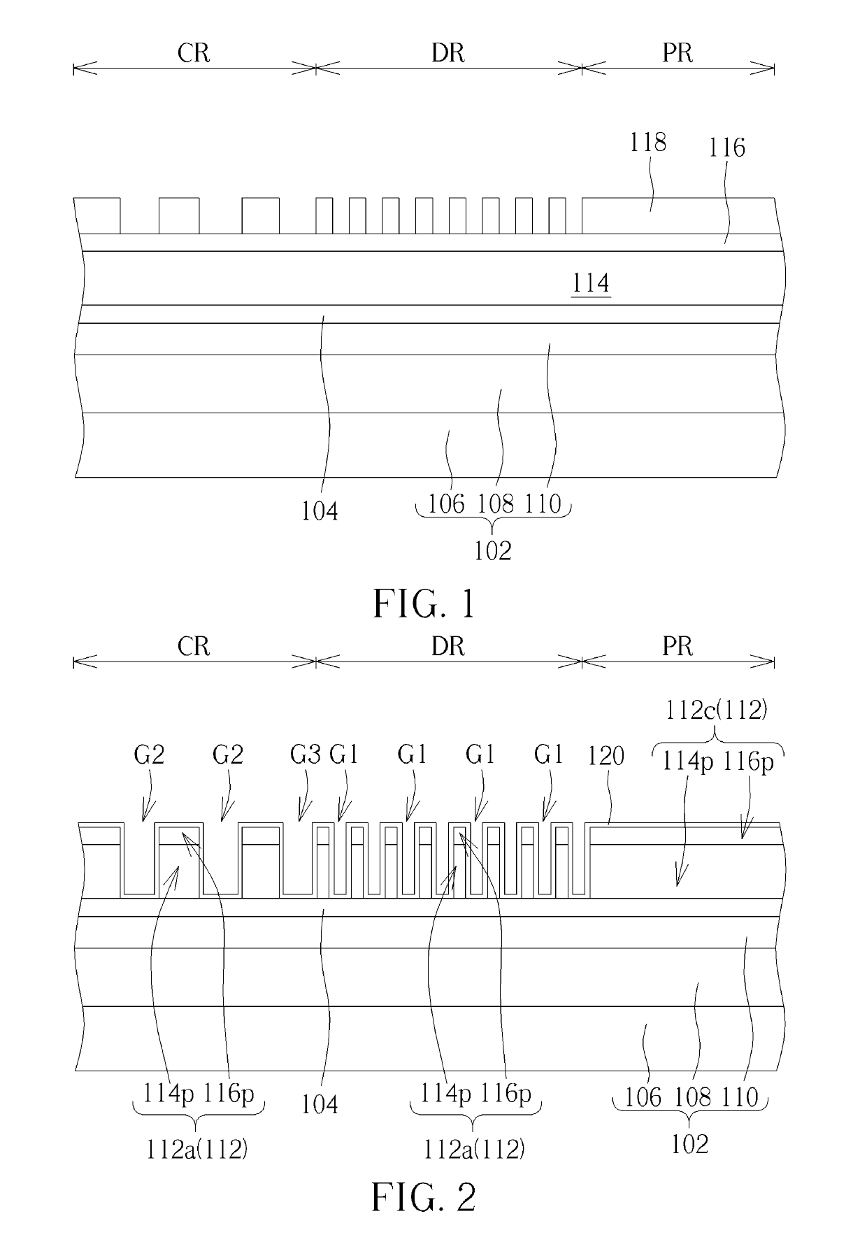
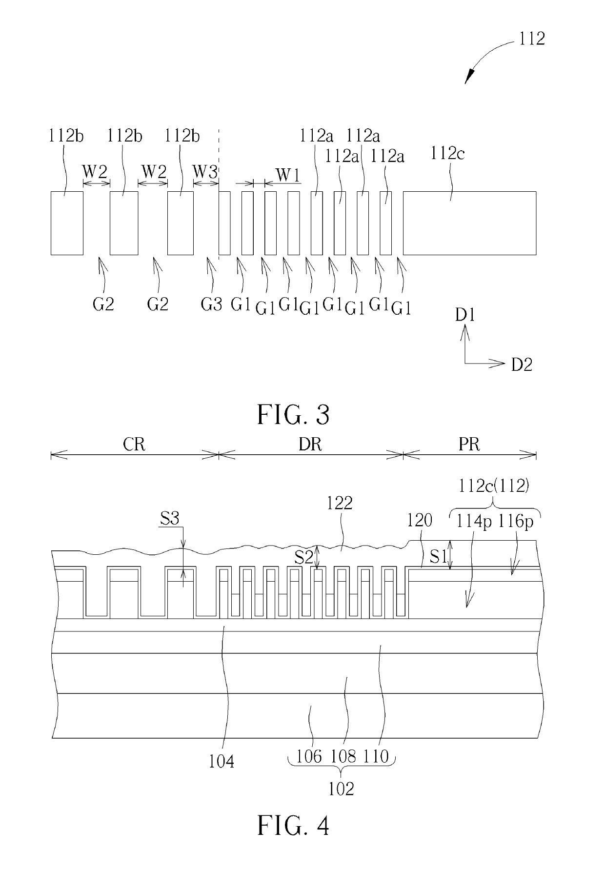
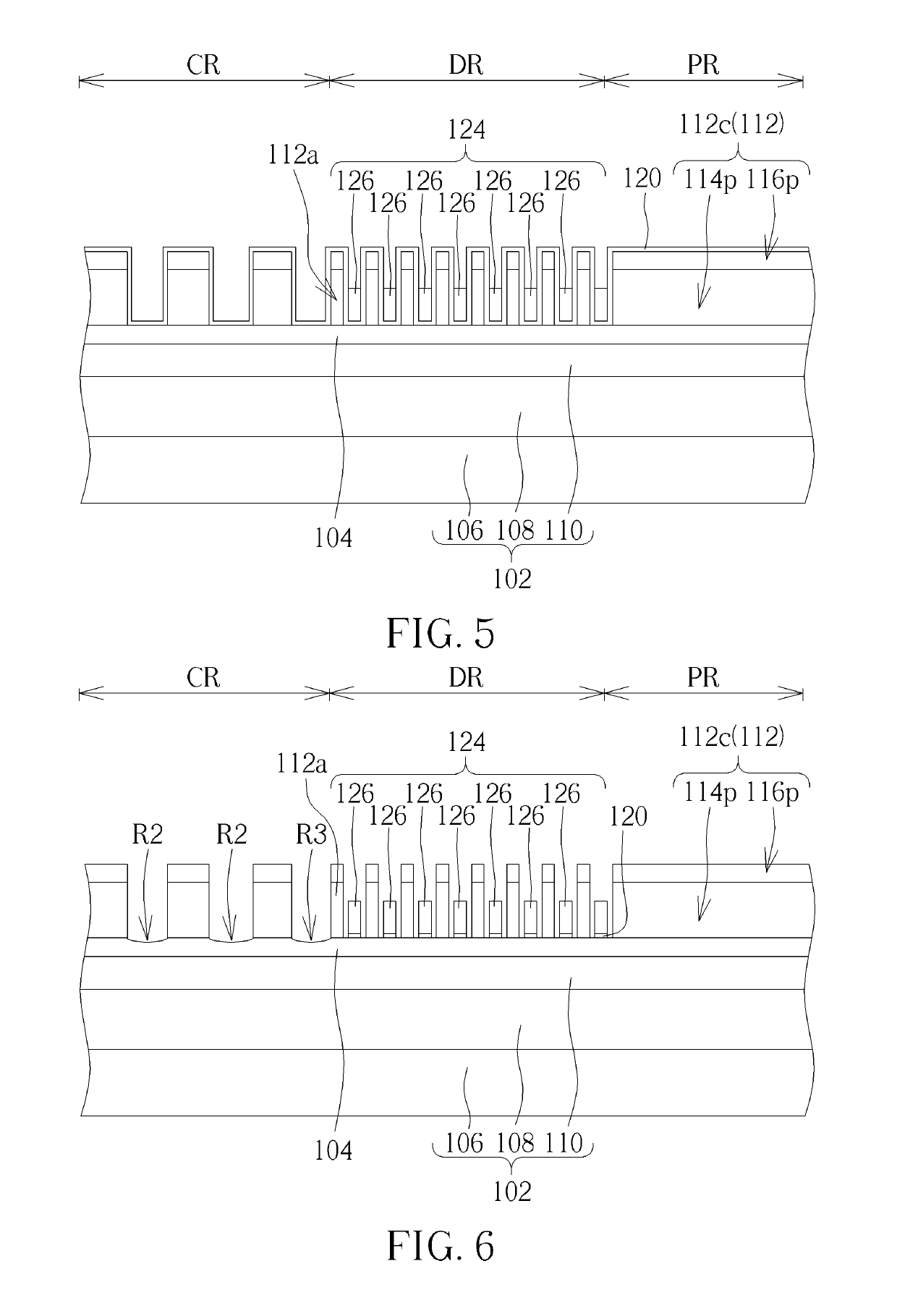
[0010]Referring to FIG. 1 to FIG. 9, FIG. 1 to FIG. 9 schematically depict a method of manufacturing a semiconductor device according to an embodiment of the present invention, in which FIG. 3 schematically illustrates a cross-sectional view of a first mask pattern according to the embodiment. First, a substrate 102, a hard mask layer 104 and a first mask pattern 112 are provided. The hard mask 104 is disposed on the substrate 102, and the first mask pattern 112 is disposed on the hard mask layer 104. Specifically, as shown in FIG. 1, the hard mask layer 104 is first formed on the substrate 102. The substrate 102 at least has a devic...


PUM

PropertyMeasurementUnit
widthaaaaaaaaaa
depthaaaaaaaaaa
sizeaaaaaaaaaa

Abstract

The present invention provides a method for manufacturing a semiconductor device including following steps. A substrate, a hard mask layer disposed on the substrate and a first mask pattern disposed on the hard mask layer are provided, and the substrate has a device region and a cutting line region. The first mask pattern has first gaps in the device region and second gaps in the cutting line region. Next, a spacer layer conformally covers the first mask pattern. Then, a second mask pattern is formed on the spacer layer in the first gaps, and a top surface of the second mask pattern is lower than a top surface of the first mask pattern. Thereafter, an etching process is performed to the spacer layer to remove the spacer layer between the first mask layer and the second mask layer and in the second gaps and expose the hard mask layer.

Description

CROSS REFERENCE TO RELATED APPLICATION[0001]The present application claims the priority benefit of Chinese patent application serial no. 201710197192.3, filed Mar. 29, 2017. The entirety of the above-mentioned patent application is hereby incorporated by reference herein.BACKGROUND OF THE INVENTION1. Field of the Invention[0002]The present invention relates to a method for manufacturing a semiconductor device, and more particularly, to a method for manufacturing a semiconductor device to increase resolution of alignment mark.2. Description of the Prior Art[0003]In semiconductor processes, in order to accurately project a pattern on a required position of a wafer, the wafer needs to be aligned before exposure, and the wafer needs alignment marks formed thereon for aligning. The alignment mark is generally aligned and detected by an optical image device, and accordingly, the accuracy and resolution of the alignment mark affect alignment error. A pattern of the alignment mark formed by...

Claims


Application Information

Patent Timeline
Patent Type & Authority Patents(United States)
IPC IPC(8): H01L21/30G03F7/09H01L23/544H01L21/308H01L21/027H01L27/105
CPCH01L21/3088G03F7/091H01L21/0276H01L21/3086H01L23/544H01L21/3085H01L2223/54426H01L27/105H01L21/0271H01L21/0273
Inventor CHEN, CHIEN-HAOWU, FENG-LUNHSIA, CHUNG-PINGLEE, SHO-SHEN
Owner UNITED MICROELECTRONICS CORP
Why Eureka
Try Eureka