Scanning drive circuit and flat display device

a drive circuit and display device technology, applied in the field of display technology, can solve the problems of affecting the output stability of the scanning drive circuit, attenuating the output capacity of the present level scanning line,

Active Publication Date: 2019-05-14
WUHAN CHINA STAR OPTOELECTRONICS TECH CO LTD
View PDF11 Cites 0 Cited by
  • Summary
  • Abstract
  • Description
  • Claims
  • Application Information

AI Technical Summary

Benefits of technology

[0003]The main technical problem of the present disclosure solved is providing a scanning drive circuit and a flat display device having the same to compensate the precharge of the pull-up control signal point, so as to ensure the output stability of the scanning drive circuit.
[0037]The beneficial effects of the present disclosure are: the situation is different from the prior art, the scanning drive circuit of the present disclosure controls the forward scan and reverse scan through the forward-reverse scanning circuit, and charging the pull-up control signal and the pull-down control signal through the input circuit, through the charge compensating circuit to compensating charge the pull-up control signal point and the pull-down control signal point, finally, output the scanning driving signal generated by the output circuit to the scan line driving the pixel unit, in order to achieve the compensation of the precharge of the scanning driving unit through the charge compensating circuit to the pull-up control signal point, thus ensuring the output stability of the scanning drive circuit.

Problems solved by technology

The existing scanning drive circuit will arranged a pull-up control signal point and a pull-down control signal point in the circuit, however, when increasing the conventional scanning drive circuit including the cascade scanning driving unit series, the upper and lower transmission signal will be attenuated, it will cause the precharge capacity of a certain level of the scanning driving unit to the pull-up control signal point insufficient, which led to the output capacity of the present level scanning line attenuated, affecting the output stability of the scanning drive circuit.

Method used


Image

  • Scanning drive circuit and flat display device
  • Scanning drive circuit and flat display device
  • Scanning drive circuit and flat display device

Examples


Embodiment Construction

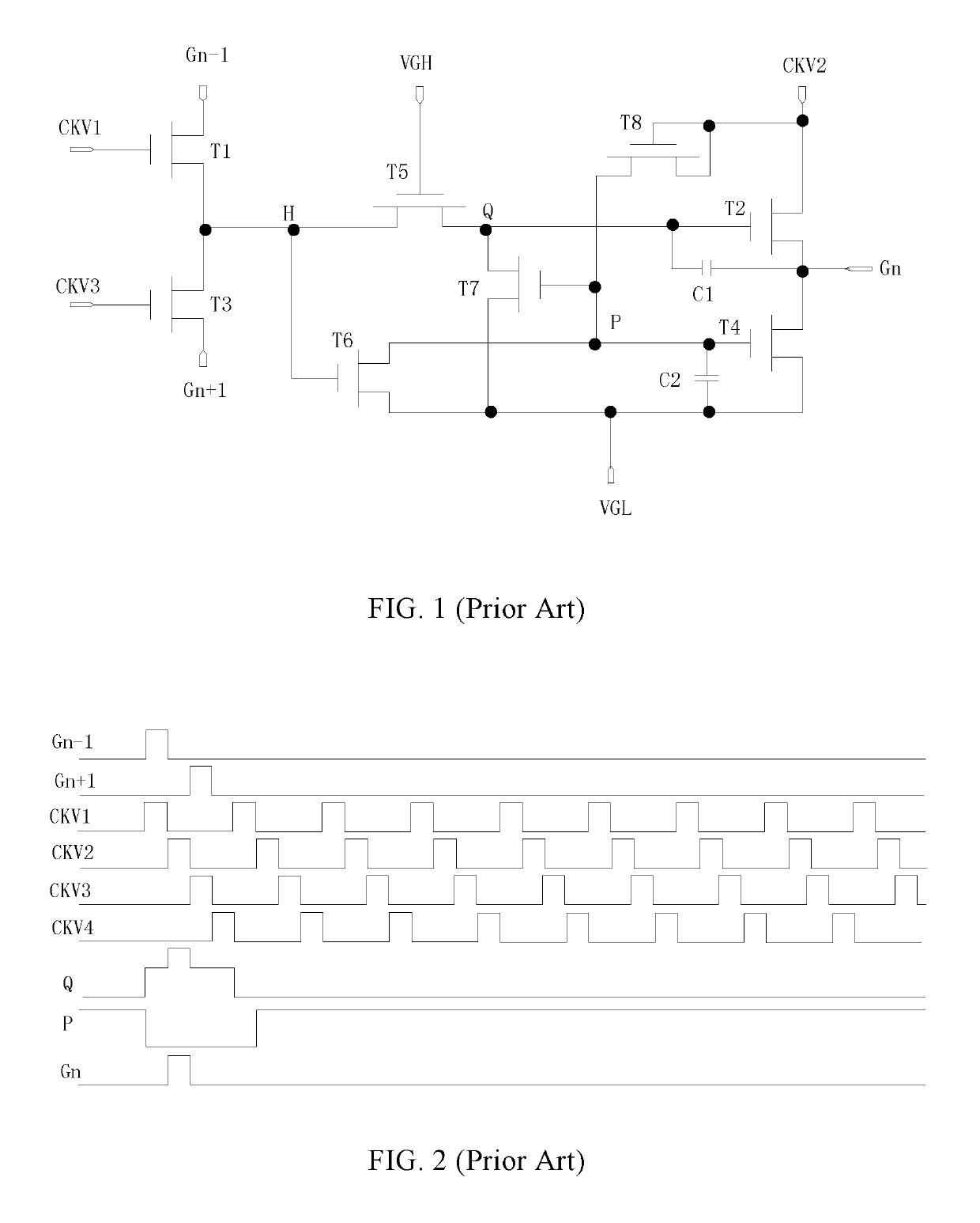
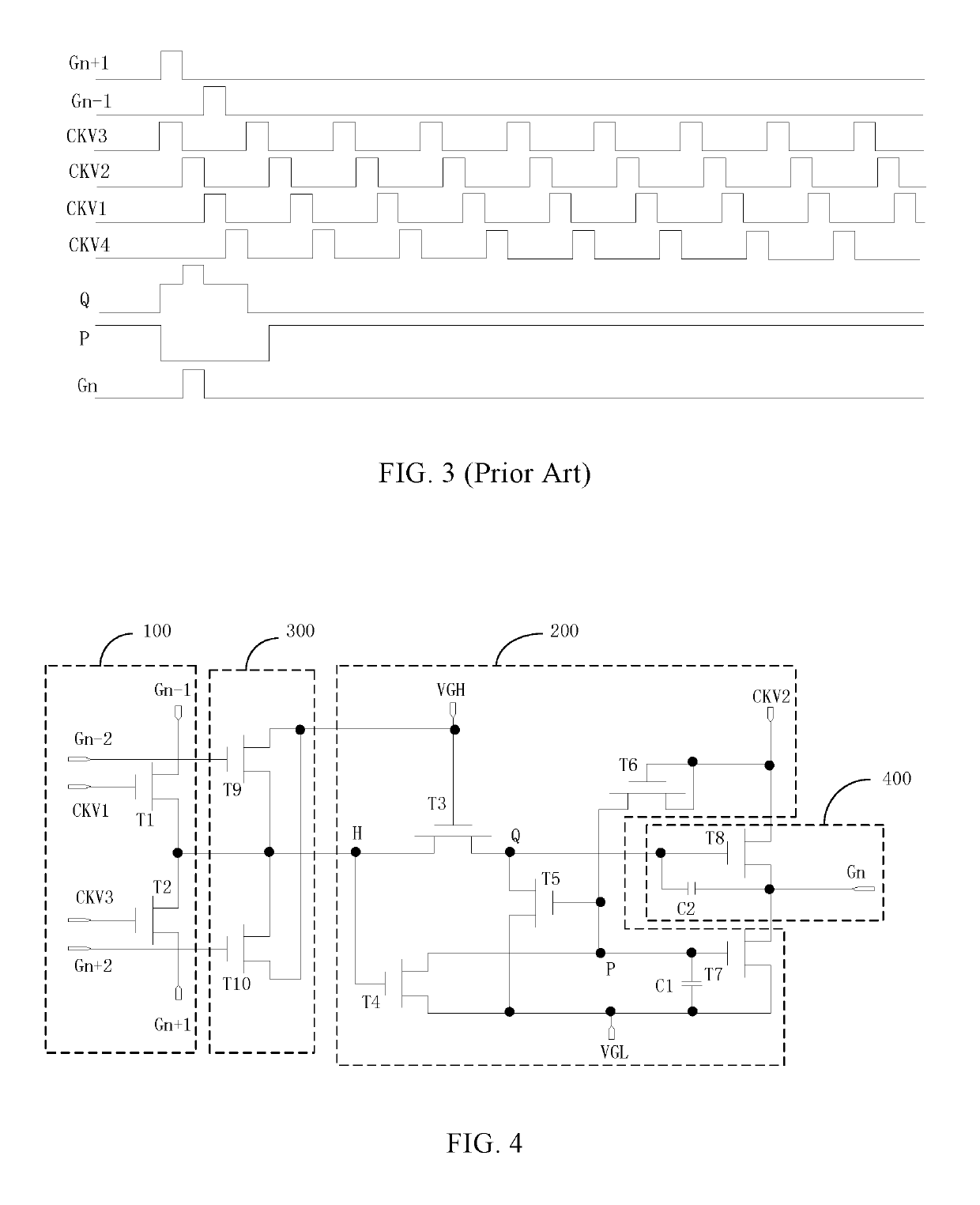
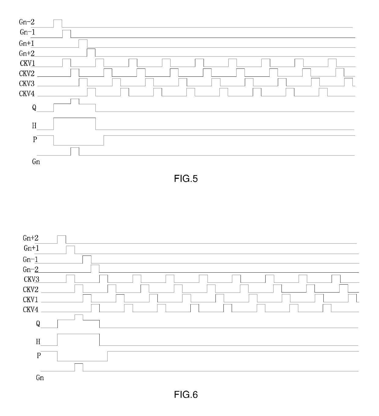
[0048]Refer to FIG. 1 and FIG. 2, the scanning drive circuit works (forward scan) in the prior art as follows:

[0049]Precharge phase: when the upper scanning signal Gn−1 and the clock signal CKV1 are high level at the same time, thin film transistor T1 is turned on and the pull-up control signal point Q is precharged, when the pull-up control signal point Q is high level, the thin film transistor T6 is in a conducting state and the pull-down control signal point P is pulled low;

[0050]The present level scanning line Gn outputting high level phase: the gate electrode of the thin film transistor T5 receives the open voltage terminal signal VGH has been in the conducting state, in the precharge phase, the pull-up control signal point Q is precharged, the capacitor C1 has a certain holding function to the charge, so that the thin film transistor T2 is in the conducting state and the high level of the clock signal CKV2 outputs to the present level scanning line Gn;

[0051]The present level s...


PUM


Abstract

The present disclosure provides a scanning drive circuit and a flat display device, the scanning drive circuit includes a plurality of cascaded scanning driving units, each scanning driving unit includes a forward-reverse scanning circuit used to control the forward scan and the reverse scan; a input circuit used to charge the pull-up and pull-down control signal point; a charge compensating circuit used to compensating charge the pull-up and pull-down control signal point; a output circuit generating the scanning driving signal to the present scanning line driving the pixel unit.

Description

FIELD OF THE DISCLOSURE[0001]The present disclosure relates to a display technology field, and more particularly to a scanning drive circuit and a flat display device having the same.BACKGROUND OF THE DISCLOSURE[0002]The current flat display device using the scanning drive circuit, which is the use of existing thin-film transistor array of flat panel display manufacturing process will formed the scanning drive circuit on the array substrate, to achieve the progressive scan drive. The existing scanning drive circuit will arranged a pull-up control signal point and a pull-down control signal point in the circuit, however, when increasing the conventional scanning drive circuit including the cascade scanning driving unit series, the upper and lower transmission signal will be attenuated, it will cause the precharge capacity of a certain level of the scanning driving unit to the pull-up control signal point insufficient, which led to the output capacity of the present level scanning lin...

Claims


Application Information

Patent Timeline
Patent Type & Authority Patents(United States)
IPC IPC(8): G09G3/3266G09G3/36G09G3/20G11C19/28
CPCG09G3/3266G09G3/20G09G3/3674G11C19/28G09G2310/0286G09G2310/0267G09G2310/0283
Inventor LI, YAFENG
Owner WUHAN CHINA STAR OPTOELECTRONICS TECH CO LTD
Why Eureka
Try Eureka