AMOLED device and manufacturing method thereof

a technology of amoled devices and manufacturing methods, which is applied in the field of display technology, can solve the problems of low manufacturing cost, large number of masks used, and extension of production time of amoled devices, and achieve the effect of reducing manufacturing costs and simplifying the manufacturing operation of amoled devices

Inactive Publication Date: 2019-05-14
TCL CHINA STAR OPTOELECTRONICS TECH CO LTD
View PDF6 Cites 0 Cited by
  • Summary
  • Abstract
  • Description
  • Claims
  • Application Information

AI Technical Summary

Benefits of technology

[0006]Objectives of the present invention are to provide a manufacturing method of an active matrix organic light-emitting diode (AMOLED) device, which uses an ink jet printing process to form an anode of the AMOLED device so as to simplify the manufacturing operation of the AMOLED device and reduce the manufacturing cost.
[0007]Objectives of the present invention are also to provide an AMOLED device, of which an anode is formed through an ink jet printing process so that the manufacturing operation is simple and the manufacturing cost is low.
[0028]The efficacy of the present invention is that the present invention provides an AMOLED device and a manufacturing method thereof. The manufacturing method of the AMOLED device according to the present invention adopts an ink jet printing operation to form an anode of the AMOLED device and thus, compared to the prior art operations, saves one mask and reduces one round of photoengraving thereby simplifying the manufacturing operation of the AMOLED device and lowering the manufacturing costs. The AMOLED device according to the present invention comprises an anode that is formed through an ink jet printing operation, so that the manufacturing operation is simplified and the manufacturing cost is reduced.

Problems solved by technology

Thus, the number of the masks used is large and the manufacturing process is complicated, leading to extension of production time of the AMOLED device and low manufacturing cost.

Method used


Image

  • AMOLED device and manufacturing method thereof
  • AMOLED device and manufacturing method thereof
  • AMOLED device and manufacturing method thereof

Examples


Embodiment Construction

[0037]To further expound the technical solution adopted in the present invention and the advantages thereof, a detailed description will be given with reference to the preferred embodiments of the present invention and the drawings thereof.

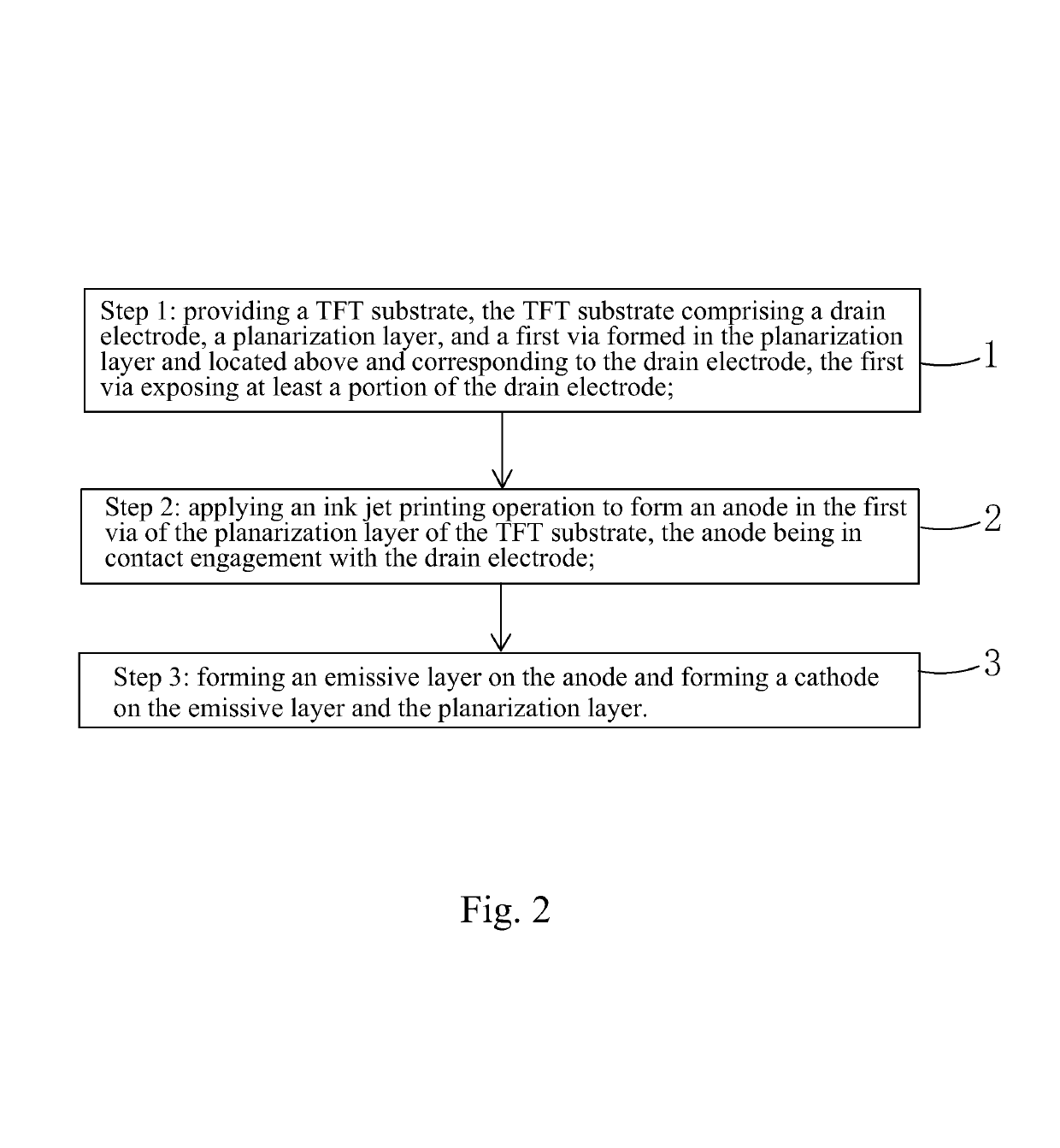
[0038]Referring to FIG. 2, firstly, the present invention provides a manufacturing method of an active matrix organic light-emitting diode (AMOLED) device, which comprises the following steps:

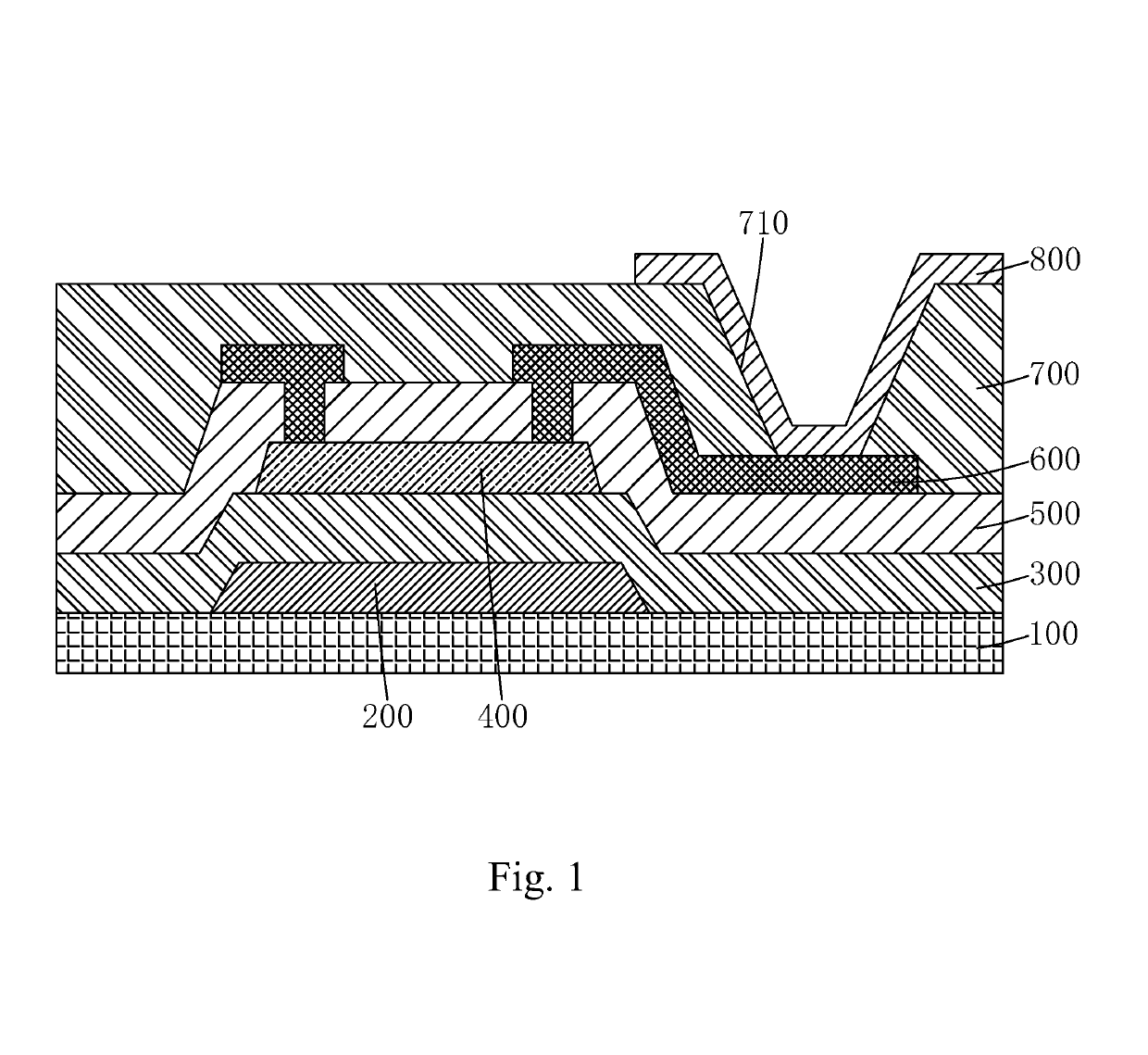
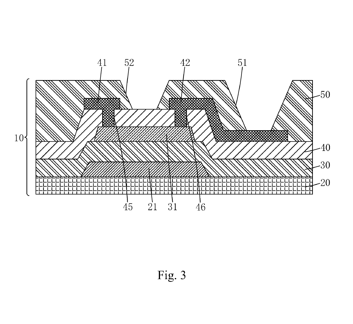
[0039]Step 1: as shown in FIG. 3, providing a thin-film transistor (TFT) substrate 10, wherein the TFT substrate 10 comprises a backing 20, a gate electrode 21 arranged on the backing 20, a gate insulation layer 30 arranged on the gate electrode 21 and the backing 20, an active layer 31 arranged on the gate insulation layer 30 and located above and corresponding to the gate electrode 21, an etch stop layer 40 arranged on the active layer 31 and the gate insulation layer 30, a source electrode 41 and a drain electrode 42 arranged on the etch stop layer 40, a p...


PUM


Abstract

The present invention provides an AMOLED device and a manufacturing method thereof. The manufacturing method of the AMOLED device according to the present invention adopts an ink jet printing operation to form an anode of the AMOLED device and thus, compared to the prior art operations, saves one mask and reduces one round of photoengraving thereby simplifying the manufacturing operation of the AMOLED device and lowering the manufacturing costs. The AMOLED device according to the present invention comprises an anode that is formed through an ink jet printing operation, so that the manufacturing operation is simplified and the manufacturing cost is reduced.

Description

BACKGROUND OF THE INVENTION1. Field of the Invention[0001]The present invention relates to the field of display technology, and more particular to an active matrix organic light-emitting diode (AMOLED) device and a manufacturing method thereof.2. The Related Arts[0002]Organic light-emitting diode (OLED) displays, which are also referred to organic electroluminescent displays, are a newly emerging flat panel display device and possess advantages, such as being self-luminous, low drive voltage, high luminous brightness, short response time, high clarity and contrast, almost 180° view angle, wide range of operation temperature, and easy realization of flexible displaying and large-area full-color displaying, and are considered the most promising display devices.[0003]Based on the way of driving, OLEDs can be classified in two categories, passive matrix OLED (PMOLED) and active matrix OLED (AMOLED), namely one for direct addressing, and the other for TFT array addressing, among which, t...

Claims


Application Information

Patent Timeline
Patent Type & Authority Patents(United States)
IPC IPC(8): H01L27/32H01L51/52H01L51/00H01L51/56H01L27/12H01L51/50
CPCH01L27/3248H01L27/1214H01L27/32H01L27/3262H01L27/3272H01L51/50H01L51/5206H01L51/56H01L51/0022H01L2251/301H01L2227/323H01L27/1259H01L27/1292H10K59/12H10K59/123H10K71/135H10K71/611H10K50/81H10K50/00H10K59/00H10K59/126H10K59/1213H10K71/00H10K59/1201H10K2102/00
Inventor HAN, BAIXIANGWU, YUANCHUN
Owner TCL CHINA STAR OPTOELECTRONICS TECH CO LTD
Why Eureka
Try Eureka