
Method for manufacturing patterned electrode and liquid crystal display panel and manufacturing method thereof

Inactive Publication Date: 2018-02-08
TCL CHINA STAR OPTOELECTRONICS TECH CO LTD
View PDF3 Cites 2 Cited by
  • Summary
  • Abstract
  • Description
  • Claims
  • Application Information

AI Technical Summary

Benefits of technology

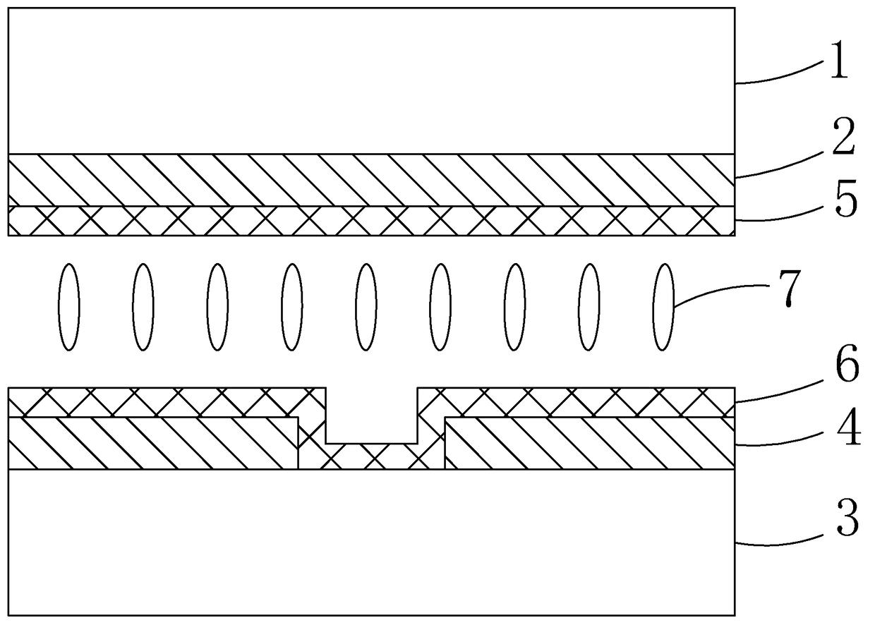
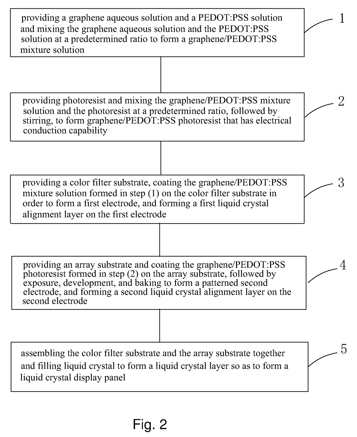
The present invention provides a method for manufacturing a patterned electrode by using a mixture of graphene, PEDOT:PSS, and photoresist. This method simplifies the manufacturing process, reduces the materials costs, and improves manufacturing efficiency. The invention also provides a manufacturing method of a liquid crystal display panel that improves product competition power by using a graphene / PEDOT:PSS mixture solution to make a complete electrode covering an entire surface, and a graphene / PEDOT:PSS photoresist that is electrically conductive to make a patterned second electrode, resulting in reduced manufacturing cost and increased manufacturing efficiency. The invention also provides a liquid crystal display panel that achieves multi-domain alignment, reduces the cost, and increases product competition power.

Problems solved by technology

However, since the VA liquid crystal panel uses liquid crystal showing the characteristics of vertical rotation and molecules of such liquid crystal have a great difference in birefringence, a relatively severe issue of color shifting of the entire panel may result.
These techniques, although quite mature, require a relatively high manufacturing cost.
Further, indium contained in ITO is a rare metal and the cost is continuously increased with the amount thereof being consumed so that the application of ITO for industrial use is constrained.
The positive photoresist has a higher cost and thus an increase of the cost for manufacturing operation results.

Method used


Image

  • Method for manufacturing patterned electrode and liquid crystal display panel and manufacturing method thereof
  • Method for manufacturing patterned electrode and liquid crystal display panel and manufacturing method thereof
  • Method for manufacturing patterned electrode and liquid crystal display panel and manufacturing method thereof

Examples


Embodiment Construction

[0036]To further expound the technical solution adopted in the present invention and the advantages thereof, a detailed description is given to a preferred embodiment of the present invention and the attached drawings.

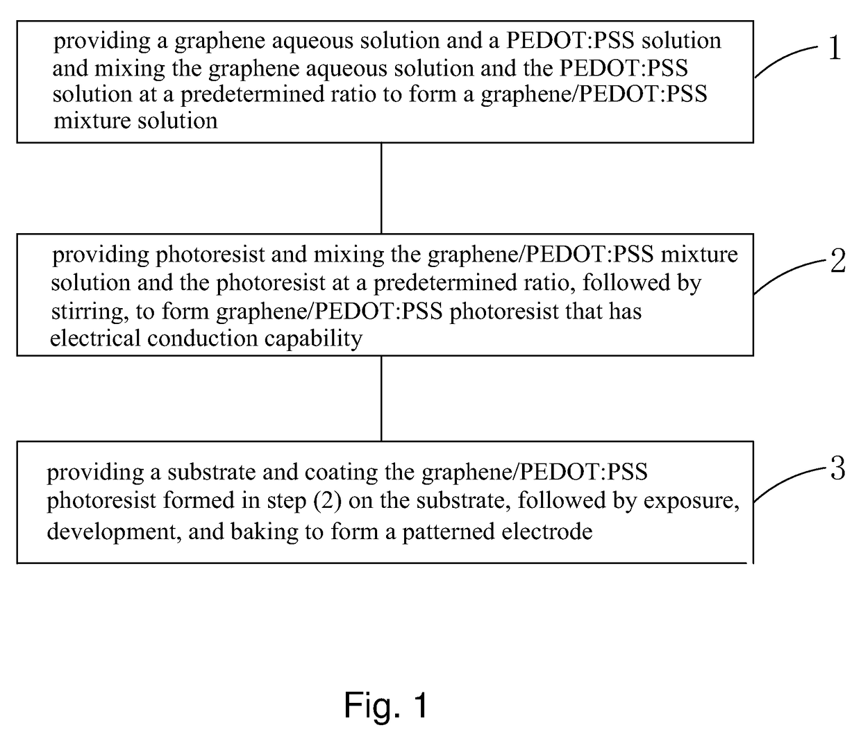
[0037]Referring to FIG. 1, firstly, the present invention provides a method for manufacturing a patterned electrode, which comprises the following steps:

[0038]Step 1: providing a graphene aqueous solution and a PEDOT:PSS (poly(3,4-ethylenedioxythiophene):polystyrene sulfonate) solution and mixing the graphene aqueous solution and the PEDOT:PSS solution at a predetermined ratio to form a graphene / PEDOT:PSS mixture solution.

[0039]Specifically, the mass percentage of graphene contained in the graphene aqueous solution is 1 wt %-99 wt %, and preferably 50 wt %.

[0040]Specifically, the mass percentage of PEDOT:PSS contained in the PEDOT:PSS solution is 1 wt %-99 wt %, and preferably 50 wt %.

[0041]Specifically, the graphene aqueous solution and the PEDOT:PSS solution are mixe...


PUM

PropertyMeasurementUnit
Temperatureaaaaaaaaaa
Timeaaaaaaaaaa

Abstract

The present invention provides a method for manufacturing a patterned electrode and a liquid crystal display panel and a manufacturing method thereof. The method for manufacturing a patterned electrode includes the following steps: Step 1: mixing a graphene aqueous solution and a PEDOT:PSS solution at a predetermined ratio to form a graphene / PEDOT:PSS mixture solution; Step 2: mixing the graphene / PEDOT:PSS mixture solution and photoresist at a predetermined ratio, followed by stirring, to form graphene / PEDOT:PSS photoresist that has electrical conduction capability; Step 3: providing a substrate and coating the graphene / PEDOT:PSS photoresist formed in Step 2 on the substrate, followed by exposure, development, and baking to form a patterned electrode. Compared to a conventional process of manufacturing an ITO electrode, the present invention can simplify the manufacturing process of a patterned electrode and lower down the manufacturing cost of the patterned electrode.

Description

BACKGROUND OF THE INVENTION1. Field of the Invention[0001]The present invention relates to the field of display technology, and in particular to a method for manufacturing a patterned electrode and a liquid crystal display panel and a manufacturing method thereof.2. The Related Arts[0002]Liquid crystal displays (LCDs) are one of the most widely used flat panel displays. A liquid crystal display panel is a key constituent part of an LCD. The liquid crystal display panel is generally composed of a color filter (CF) substrate, a thin-film transistor (TFT) array substrate, and a liquid crystal layer arranged between the two substrates. Generally, the array substrate and the CF substrate are respectively provided with a pixel electrode and a common electrode. When an electrical voltage is applied between the pixel electrode and the common electrode to induce an electric field, the electric field determines the orientation of liquid crystal molecules and thus adjusting polarization of lig...

Claims


Application Information

Patent Timeline
IPC IPC(8): G02F1/1343
CPCG02F1/13439G02F2201/121G02F2201/123G02F2202/16G02F2203/01G02F1/1333G02F2202/022H10K71/621H10K85/1135
Inventor LEE, YUNGJUIWANG, HAIJUNHU, TAO
Owner TCL CHINA STAR OPTOELECTRONICS TECH CO LTD
Learn More