IPS thin-film transistor array substrate and manufacturing method thereof

a technology of thin-film transistors and array substrates, applied in the field of display technology, can solve the problems of high fabrication cost of masks, long time period of fabrication of ips tft array substrates, and complex manufacturing process, and achieve the effect of reducing the number of mask-involved operations and low manufacturing cos

Active Publication Date: 2021-09-07
SHENZHEN CHINA STAR OPTOELECTRONICS SEMICON DISPLAY TECH CO LTD
View PDF4 Cites 0 Cited by
  • Summary
  • Abstract
  • Description
  • Claims
  • Application Information

AI Technical Summary

Benefits of technology

[0006]Objectives of the present invention are to provide a method for manufacturing an in-plane switching (IPS) thin-film transistor (TFT) array substrate, which includes a reduced number of mask-involved operations and has a low manufacturing cost.
[0007]Objectives of the present invention are also to provide an IPS TFT array substrate, which has a simple manufacturing operation and a low manufacturing cost and demonstrates excellent electrical properties.
[0048]The efficacy of the present invention is that the method for manufacturing an IPS TFT array substrate according to the present invention can be done with only three mask-involved operations. Compared to the state of the art, the number of masks used is reduced, the manufacturing time is shortened, and thus the manufacturing cost is lowered. The IPS TFT array substrate of the present invention that is manufactured with the above method has a simple manufacturing process, a low manufacturing cost, and excellent electrical properties.

Problems solved by technology

Since the masks have a high fabrication cost and a process including multiple mask-involved operations needs an extended time period of fabrication.
Thus, the fabrication cost of the IPS TFT array substrate is relatively high.

Method used


Image

  • IPS thin-film transistor array substrate and manufacturing method thereof
  • IPS thin-film transistor array substrate and manufacturing method thereof
  • IPS thin-film transistor array substrate and manufacturing method thereof

Examples


Embodiment Construction

[0071]To further expound the technical solution adopted in the present invention and the advantages thereof, a detailed description will be given with reference to the preferred embodiments of the present invention and the drawings thereof.

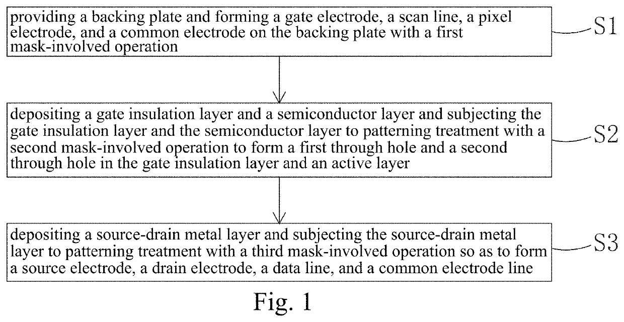
[0072]Referring to FIG. 1, the present invention provides a method for manufacturing an in-plane switching (IPS) thin-film transistor (TFT) array substrate, which comprises the following steps:

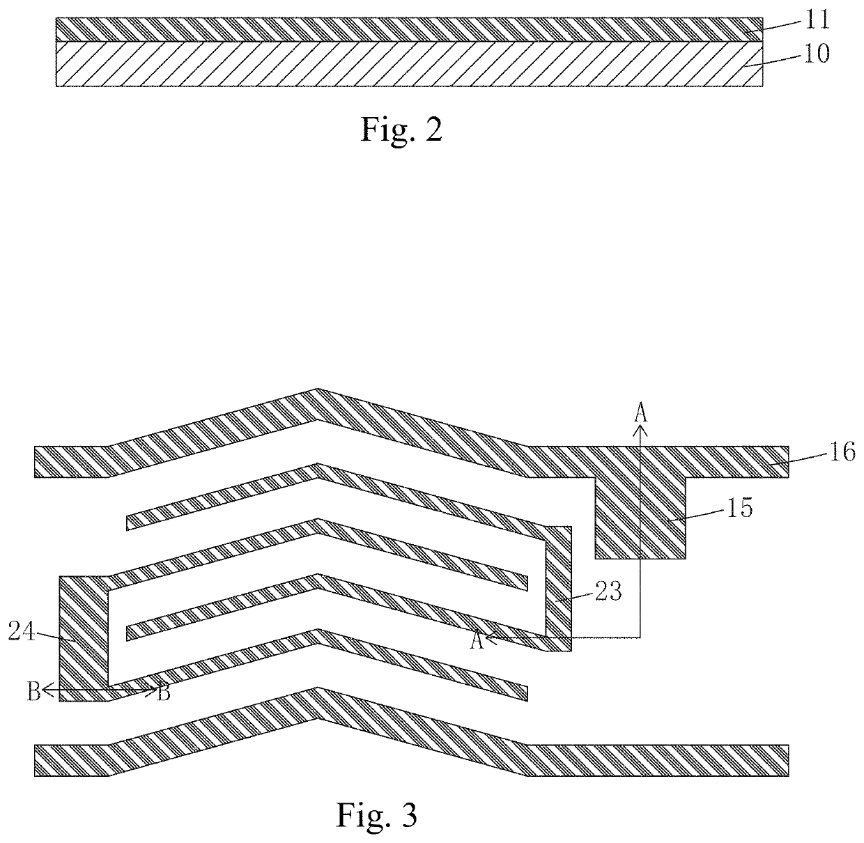
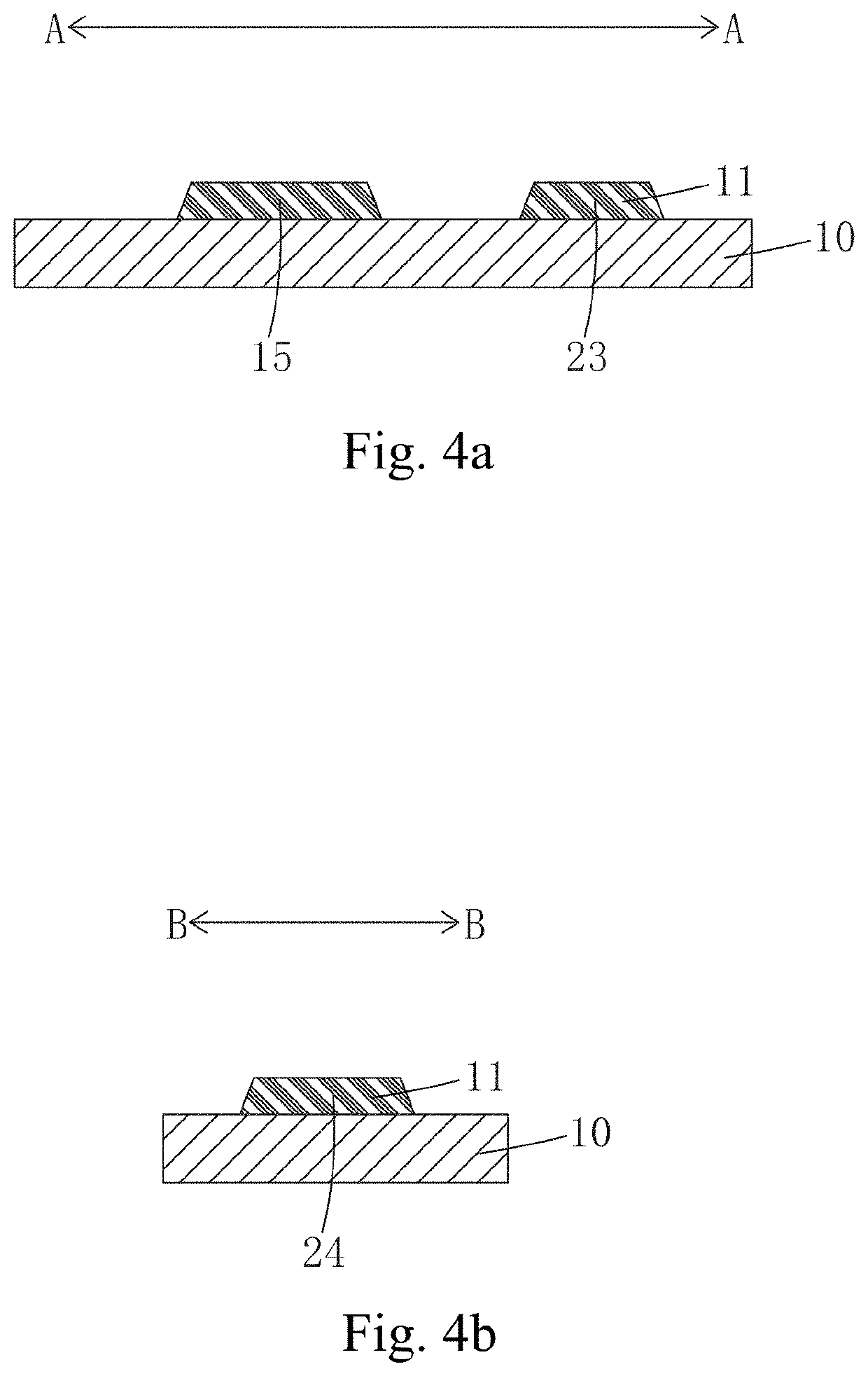
[0073]S1: as shown in FIGS. 2-6b, providing a backing plate 10 and forming a gate electrode 21, a scan line 22, a pixel electrode 23, and a common electrode 24 on the backing plate 10 with a first mask-involved operation, wherein the scan line 22 and the gate electrode 21 are connected to each other.

[0074]Specifically, Step S1 comprises:

[0075]S11: as shown in FIG. 2, depositing a first metal layer 11 on the backing plate 10 with physical vapor deposition (PVD);

[0076]S12: as shown in FIGS. 3, 4a, and 4b, subjecting the first metal layer 11 to patterning treat...


PUM

PropertyMeasurementUnit
light transmittanceaaaaaaaaaa
electrical conductanceaaaaaaaaaa

Abstract

The present invention provides an IPS TFT array substrate and a manufacturing method thereof. The manufacturing method of an IPS TFT array substrate of the present invention includes: forming a gate electrode, a scan line, a pixel electrode, and a common electrode with a first mask-involved operation, forming a first through hole and a second through hole in the gate insulation layer and an active layer with a second mask-involved operation, and forming a source electrode, a drain electrode, a data line, and a common electrode line with a third mask-involved operation. The present invention uses only three mask-involved operations to complete the manufacturing of an IPS TFT array substrate. Compared to the state of the art, the number of masks used is reduced, the manufacturing time is shortened, and thus the manufacturing cost is lowered. The IPS TFT array substrate of the present invention has a simple manufacturing process, a low manufacturing cost, and excellent electrical properties.

Description

BACKGROUND OF THE INVENTION1. Field of the Invention[0001]The present invention relates to the field of display technology, and more particular to an in-plane switching (IPS) thin-film transistor (TFT) array substrate and a manufacturing method thereof.2. The Related Arts[0002]With the progress of the display technology, liquid crystal displays (LCDs), due to various advantages, such as high image quality, low power consumption, thin device body, and wide range of applications, have been widely used in all sorts of consumer electronic products, including mobile phones, televisions, personal digital assistants (PDAs), digital cameras, notebook computers, and desktop computers, and are becoming a main stream of the display devices.[0003]Most of the liquid crystal display devices that are currently available in the market are backlighting LCDs, which comprise a liquid crystal panel and a backlight module.[0004]The liquid crystal display panel is generally made up of a color filter (CF)...

Claims


Application Information

Patent Timeline
Patent Type & Authority Patents(United States)
IPC IPC(8): H01L27/12G02F1/1362G02F1/1343G02F1/1368
CPCH01L27/1288G02F1/1368G02F1/13439G02F1/134363G02F1/136227G02F1/136286H01L27/124H01L27/1259G02F1/134318G02F1/136236G02F1/136295G02F2201/121G02F2201/123G02F2201/124
Inventor ZHOU, ZHICHAOXIA, HUICHEN, MENG
Owner SHENZHEN CHINA STAR OPTOELECTRONICS SEMICON DISPLAY TECH CO LTD
Why Eureka
Try Eureka