Array substrate, liquid crystal display panel and manufacturing method for array substrate

a technology of array substrate and liquid crystal display panel, which is applied in the field of array substrate, can solve the problems of image sticking (is), panel generation of crosstalk problem, price cost and production time cost increase, etc., and achieve the effect of increasing the number of masks and affecting production capacity

Inactive Publication Date: 2019-05-21
TCL CHINA STAR OPTOELECTRONICS TECH CO LTD
View PDF17 Cites 0 Cited by
  • Summary
  • Abstract
  • Description
  • Claims
  • Application Information

AI Technical Summary

Benefits of technology

[0008]The technology problem mainly solved by the present invention is to provide an array substrate, a liquid crystal display panel and a manufacturing method for an array substrate such that the a-Si below the data line will not be irradiated by a light in order to avoid a photo-leakage current problem without increasing the number of the masks and affecting the production capacity at the same time.

Problems solved by technology

The panel generates a crosstalk problem and an Image Sticking (IS) problem caused by the photo-leakage current.
If using a non-metal material to manufacture a light shielding layer, the price cost and the production time cost will increase.

Method used


Image

  • Array substrate, liquid crystal display panel and manufacturing method for array substrate
  • Array substrate, liquid crystal display panel and manufacturing method for array substrate
  • Array substrate, liquid crystal display panel and manufacturing method for array substrate

Examples


Embodiment Construction

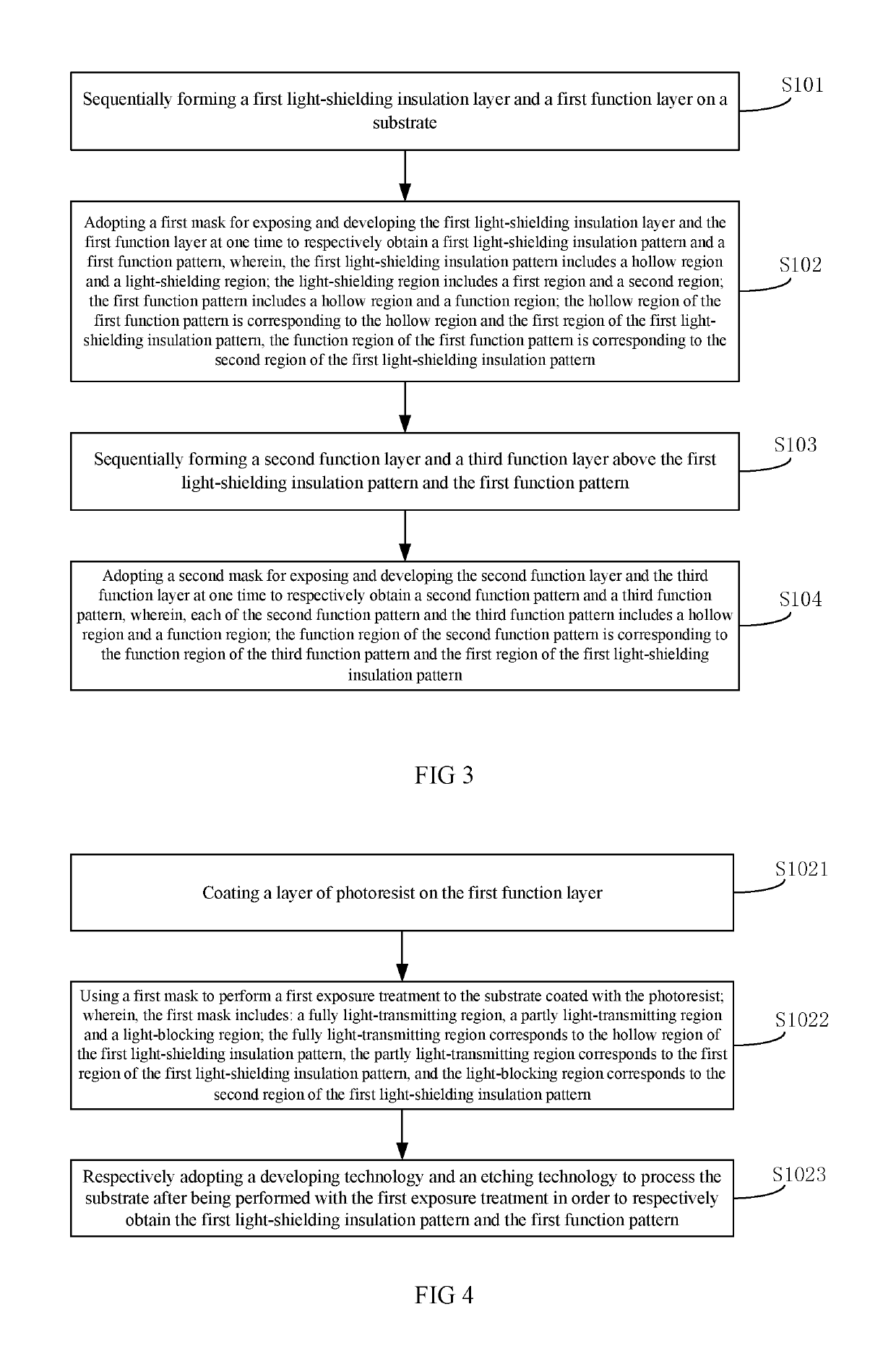
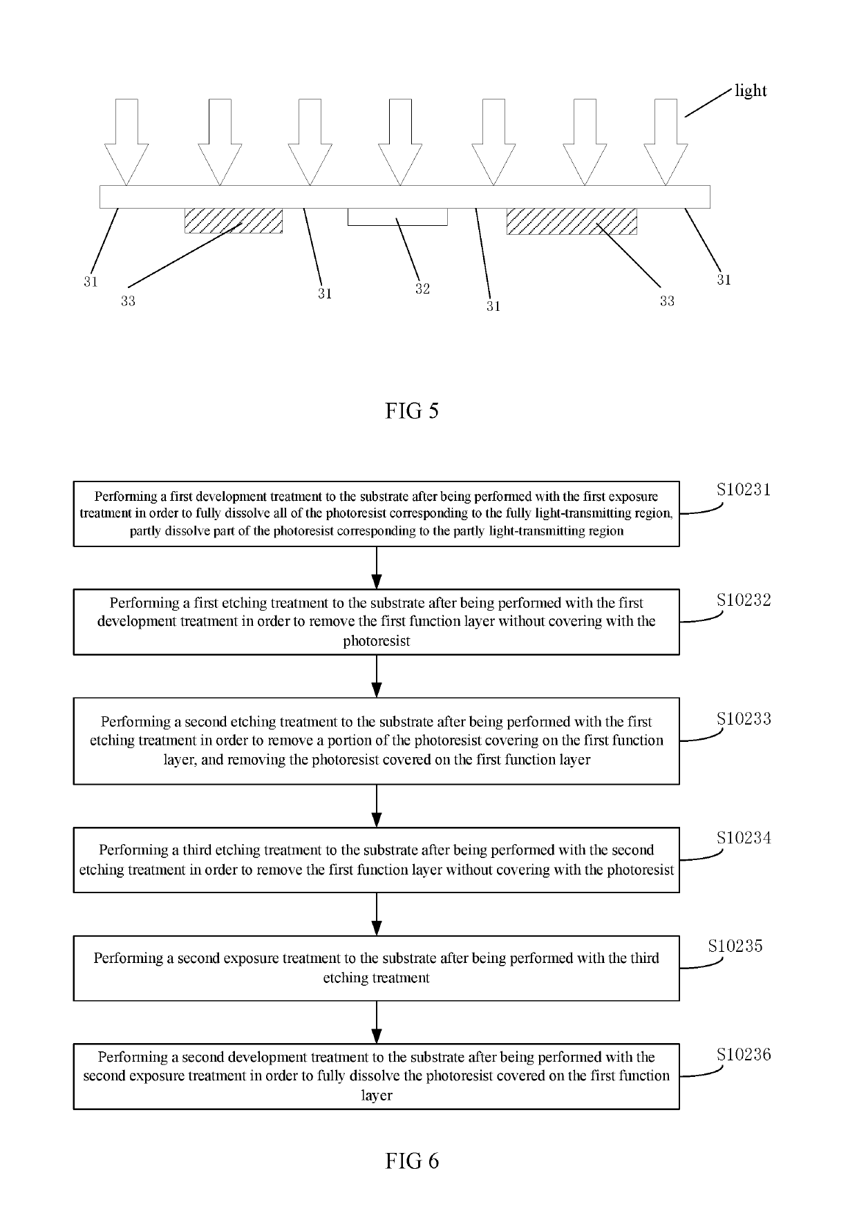
[0064]The following content combines with the drawings and the embodiment for describing the present invention in detail.

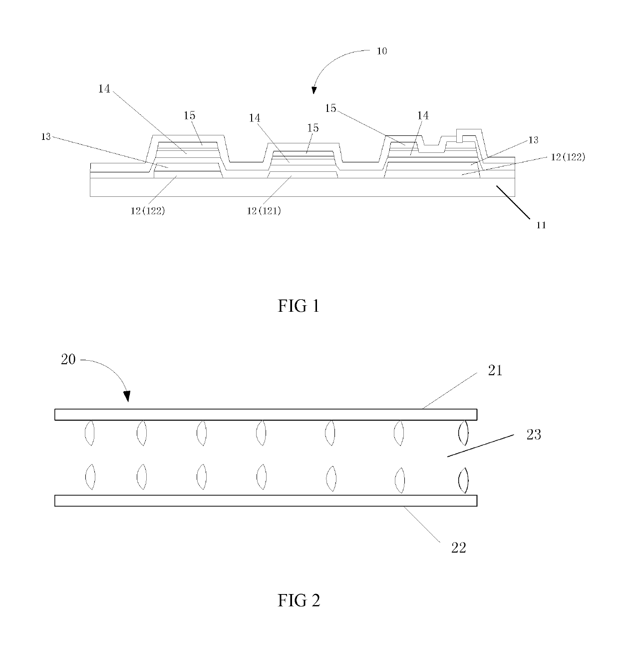
[0065]With reference to FIG. 1, and FIG. 1 is a schematic diagram of an array substrate of an embodiment of the present invention. The array substrate 10 includes: a substrate 11, a first light-shielding insulation layer 12, a first function layer 13, a second function layer 14 and a third function layer 15.

[0066]The first light-shielding insulation layer 12 is formed on the substrate 11, used for blocking a portion of light entering to the substrate 11, and the first light-shielding insulation layer 12 includes: a first region 121 and a second region 122 disposed separately, and the first region 121 and the second region 122 are both made of an insulation material such as a plastic material or a black matrix material.

[0067]The first function layer 13 is formed on the second region 122 of the first light-shielding insulation layer 12, used for realizing a first fu...


PUM

PropertyMeasurementUnit
light-shieldingaaaaaaaaaa
light-shielding aaaaaaaaaa
semiconductoraaaaaaaaaa

Abstract

An array substrate includes a first light-shielding insulation layer formed on the substrate, for block a light entering the substrate, and including a first region and a second region, and each is made of an insulation material; a first function layer formed on the second region, under a light-shielding function of the second region, an affection of light is avoided; a second function layer formed above the first region of the first light-shielding insulation layer and the first function layer, under the light-shielding function of the first light-shielding insulation layer, an affection of light is avoided; and a third function layer formed above the second function layer, under the light-shielding function of the first light-shielding insulation layer, an affection of light is avoided; wherein, each of the first, the second and the third function layer is a conductor material or a semiconductor material. A photo-leakage current can be avoided.

Description

BACKGROUND OF THE INVENTION[0001]1. Field of the Invention[0002]The present invention relates to a liquid crystal display field, and more particularly to an array substrate, a liquid crystal display panel and a manufacturing method for array substrate.[0003]2. Description of Related Art[0004]In the production of a Thin Film Transistor-Liquid Crystal Display (abbreviated as TFT-LCD), the current main technology is adopting five masks, that is, a five-mask process. In order to decrease the cost, the current research direction is decreasing the number of the masks.[0005]Currently, many productions adopt four masks, that is, a four-mask process. The four-mask process generally combines an a-Si (abbreviated as AS) layer and a source electrode (abbreviated as SE) in the five masks to be one mask. The one mask adopts a Gray Tone Mask (GTM) technology or a Half Tone Mask (HTM) technology to perform a process. In the five-mask process, the a-Si layer only exists at a channel region. For a fo...

Claims


Application Information

Patent Timeline
Patent Type & Authority Patents(United States)
IPC IPC(8): G02F1/1368G02F1/1362G02F1/1333H01L27/12
CPCG02F1/1368G02F1/1362G02F1/133345G02F1/136209H01L27/12G02F2001/13625G02F2001/136236G02F2202/103H01L23/552H01L27/1214G02F1/136295H01L29/78633H01L27/124H01L27/1255H01L27/1288G02F1/136236G02F1/13625
Inventor ZHANG, MENGMENG
Owner TCL CHINA STAR OPTOELECTRONICS TECH CO LTD
Why Eureka
Try Eureka