Semiconductor Device and Manufacturing Method Thereof
- Summary
- Abstract
- Description
- Claims
- Application Information
AI Technical Summary
Benefits of technology
Problems solved by technology
Method used
Image

Examples
embodiment 1
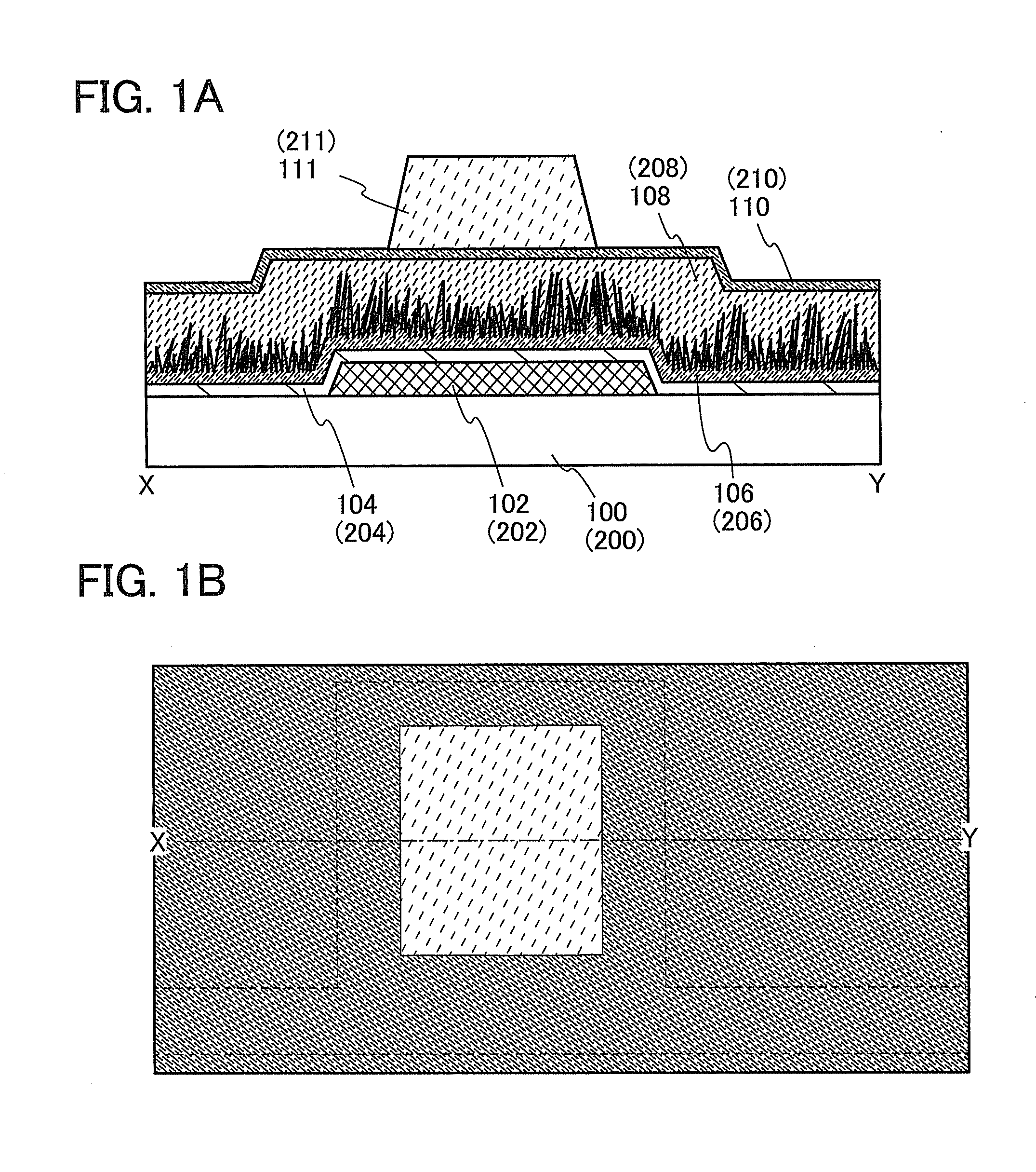
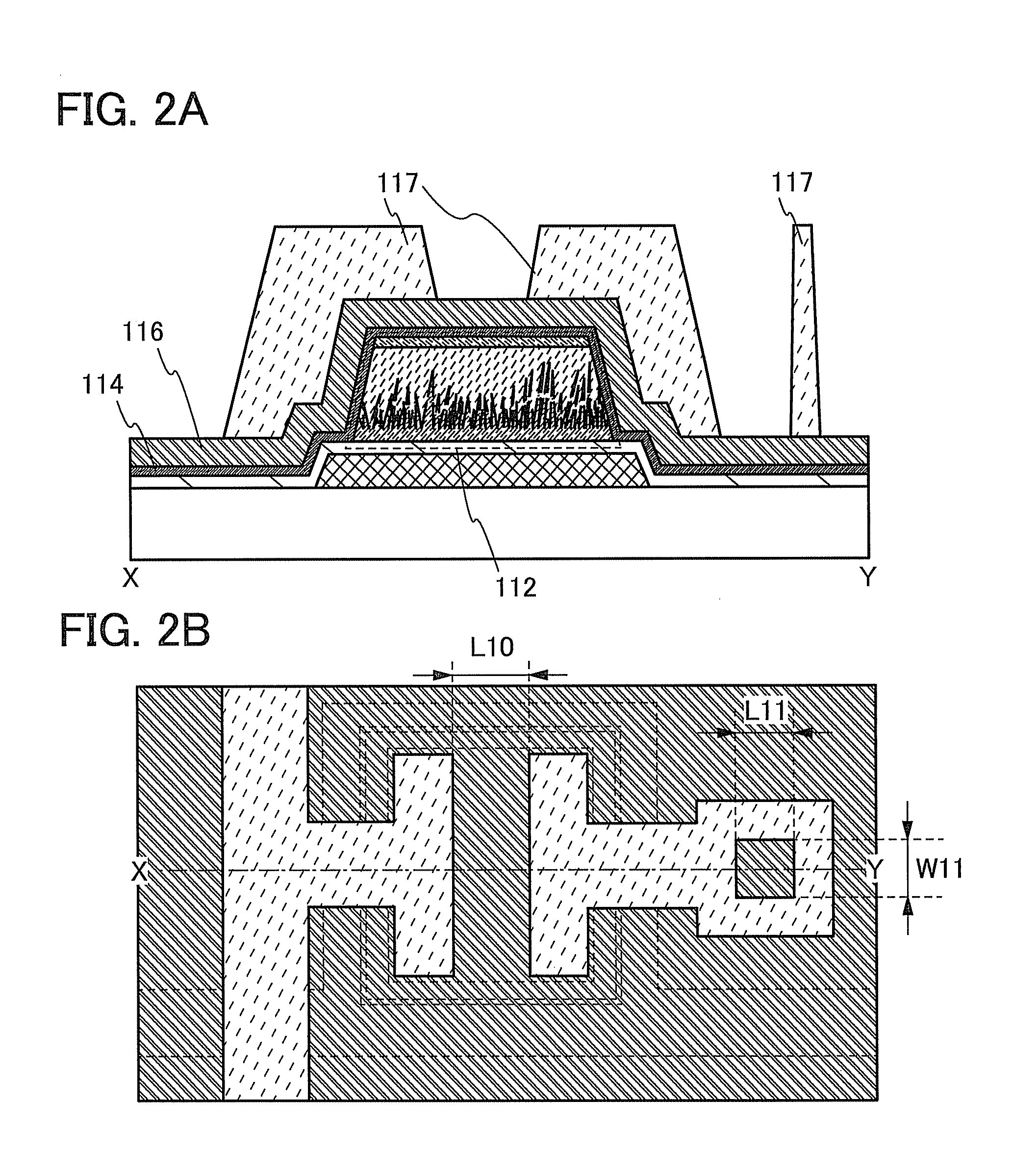
[0049]In this embodiment, a semiconductor device that is one embodiment of the present invention and a manufacturing method thereof are described. Note that in the following description, FIG. 1A, FIG. 2A, FIG. 3A, FIG. 4A, FIG. 5A, FIG. 6A, and FIG. 7A are cross-sectional views taken along line X-Y in FIG. 1B, FIG. 2B, FIG. 3B, FIG. 4B, FIG. 5B, FIG. 6B, and FIG. 7B, respectively.
[0050]First, a first conductive layer 102 is formed over a substrate 100, and a first insulating layer 104 is formed so as to cover the first conductive layer 102. Next, a first semiconductor film 106, a second semiconductor film 108, and an impurity semiconductor film 110 are stacked in this order over the first insulating layer 104, and an etching mask 111 is formed over the impurity semiconductor film 110 (FIGS. 1A and 1B).
[0051]The substrate 100 is an insulating substrate. As the substrate 100, in addition to a glass substrate, a quartz substrate, and a ceramic substrate, a plastic substrate or the like...
embodiment 2
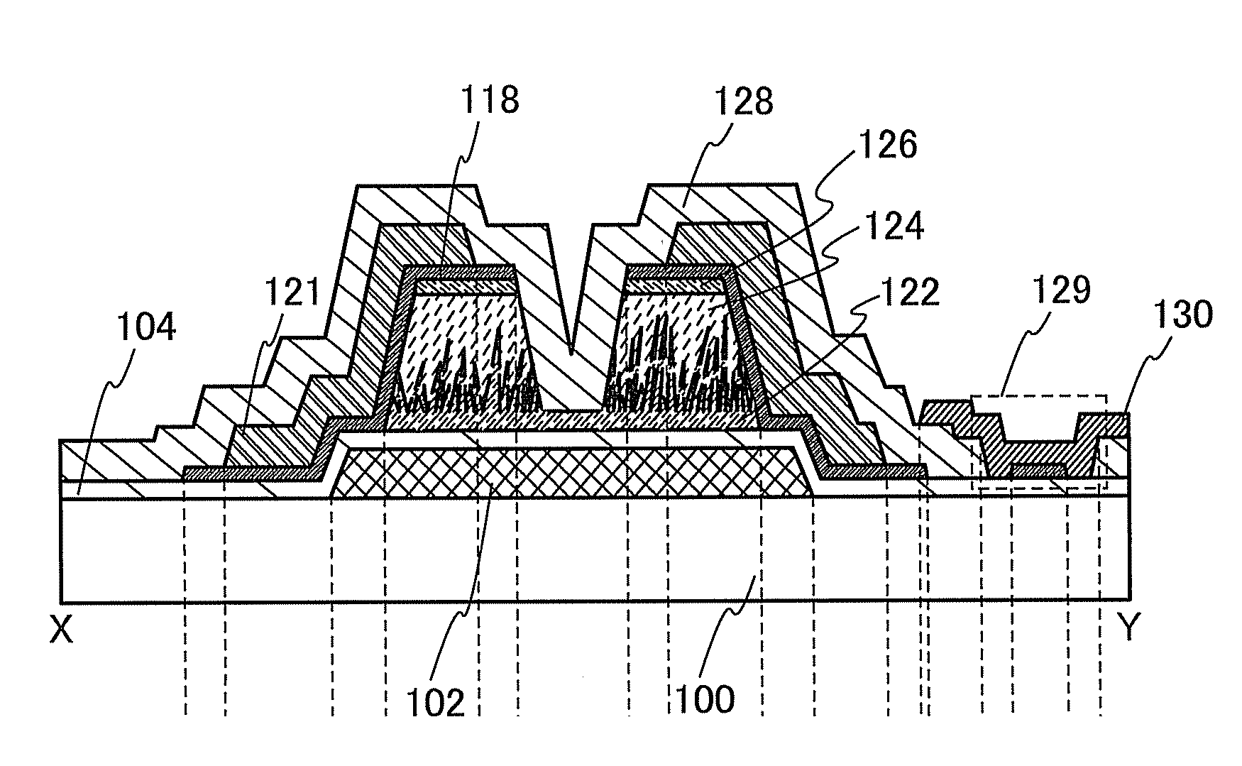
[0107]In this embodiment, a semiconductor device that is one embodiment of the present invention and a manufacturing method thereof are described. Specifically, a semiconductor device in which a plurality of openings is formed and a manufacturing method thereof are described. Note that in the following description, FIG. 1A, FIG. 10A, FIG. 11A, FIG. 12A, FIG. 13A, FIG. 14A, and FIG. 15A are cross-sectional views taken along line X-Y in FIG. 1B, FIG. 10B, FIG. 11B, FIG. 12B, FIG. 13B, FIG. 14B, and FIG. 15B, respectively.
[0108]First, as in Embodiment 1, a first conductive layer 202 is formed over a substrate 200, and a first insulating layer 204 is formed so as to cover the first conductive layer 202. Next, a first semiconductor film 206, a second semiconductor film 208, and an impurity semiconductor film 210 are stacked in this order over the first insulating layer 204, and an etching mask 211 is formed over the impurity semiconductor film 210 (FIGS. 1A and 1B). Note that in FIG. 1A,...
embodiment 3
[0154]As a semiconductor device to which the thin film transistor described in Embodiment 1 or Embodiment 2 is applied, an electronic paper is given. An electronic paper can be used for electronic appliances of a variety of fields as long as they can display data. For example, electronic paper can be applied to an electronic book reader (e-book), a poster, a digital signage, a public information display (PID), an advertisement in a vehicle such as a train, displays of various cards such as a credit card, and the like. FIG. 18 illustrates an example of the electronic appliances.
[0155]FIG. 18 illustrates an example of an electronic book reader. For example, an electronic book reader 300 includes two housings 301 and 303. The housing 301 and the housing 303 are combined with a hinge 311 so that the electronic book reader 300 can be opened and closed with the hinge 311 as an axis. With such a structure, the electronic book reader 300 can be handled like a paper book.
[0156]A display port...
PUM
 Abstract
Description
Claims
Application Information
 - R&D Engineer
- R&D Manager
- IP Professional
- Industry Leading Data Capabilities
- Powerful AI technology
- Patent DNA Extraction
Browse by: Latest US Patents, China's latest patents, Technical Efficacy Thesaurus, Application Domain, Technology Topic.
© 2024 PatSnap. All rights reserved.Legal|Privacy policy|Modern Slavery Act Transparency Statement|Sitemap