Manufacturing method of mems device and mems device

A manufacturing method and device technology, applied in the manufacture of MEMS devices and the field of MEMS devices, can solve the problems that the film area cannot be made larger, the contact hole cannot be made smaller, and the performance of the device is affected, so as to achieve more convenience and feasibility, form The method is flexible and the effect of improving device performance

Active Publication Date: 2021-05-14
SEMICON MFG ELECTRONICS (SHAOXING) CORP
View PDF7 Cites 0 Cited by
  • Summary
  • Abstract
  • Description
  • Claims
  • Application Information

AI Technical Summary

Problems solved by technology

However, with the development of technology, the size of the device is getting smaller and smaller, and the design size of the contact hole and the contact pad is limited, resulting in a small area of ​​the film layer covering the periphery of the contact hole by the contact pad 104a, 104b. Etching solution may seep into the bottom of the contact hole from the edge of the contact pad 104a, 104b, and cause the polysilicon layer (that is, a part of the upper plate 103) at the bottom of the contact hole to be electrochemically corroded, thereby affecting the performance of the device
[0005] In addition, due to the limitation of device design requirements, the contact hole cannot be made small, and the area of ​​the film layer around the contact hole cannot be made large. When the size of the contact hole remains unchanged, the size of the contact hole and the contact pad cover the film layer around the contact hole. Obviously, when the size of the contact hole remains the same, it is impossible to increase the area of ​​the contact pad covering the periphery of the contact hole by reducing the size of the contact hole, so as to prevent the wet etching solution from penetrating into the contact hole. bottom

Method used


Image

  • Manufacturing method of mems device and mems device
  • Manufacturing method of mems device and mems device
  • Manufacturing method of mems device and mems device

Examples


Embodiment approach

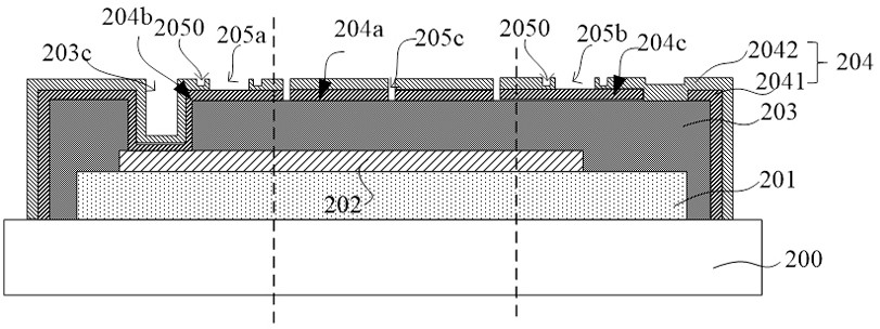
[0067] In addition, although this embodiment shows that the upper plate material layer 204 is composed of three layers, and the bottom dielectric layer 2043 is reserved at the bottom of the groove 203b, the technical solution of the present invention is not limited thereto . In other embodiments of the present invention, when the method of forming the groove 203b in the first insulating dielectric layer is used to solve the problem of electrochemical corrosion of the conductive layer 2041 below due to the infiltration of etching solution at the contact hole of the upper plate lead-out part 204c When there is a problem, as long as the upper plate lead-out portion 204c does not cause a short circuit between the upper plate 204a and the lower plate 202, the bottom dielectric layer 2043 can be omitted in the upper plate material layer 204, or the upper plate lead-out portion The conductive layer 2041 of 204c is in direct contact with the corresponding portion of the lower plate 20...


PUM


Abstract

The invention provides a method for manufacturing a MEMS device and the MEMS device, wherein an annular barrier structure is formed on the upper surface of the upper plate material layer at the periphery of at least one contact hole of the plate lead-out part, and the annular barrier structure includes a protrusion and / or a groove, the corresponding contact pad is filled in the contact hole and extends to the annular barrier structure, and at least covers the side wall of the ring-shaped barrier structure on the side away from the contact hole or at least covers the ring-shaped barrier structure The groove of the barrier structure is close to the side wall of one side of the contact hole, thus on the one hand, the ring-shaped barrier structure is used to increase the contact area between the edge of the contact pad and the lower film layer, and on the other hand, the ring-shaped barrier structure is used to make the contact The edge of the pad is undulating, therefore, the contact pad can prevent the wet etching solution from penetrating into the bottom of the contact hole, prevent the material at the bottom of the contact hole from being electrochemically corroded, and improve device performance.

Description

technical field [0001] The invention relates to the technical field of integrated circuit manufacturing, in particular to a method for manufacturing a MEMS device and the MEMS device. Background technique [0002] With the development of technology, MEMS (Micro-Electro-Mechanical System, Micro-Electro-Mechanical System) devices, such as microphones, miniaturized inertial sensors, pressure sensors, acceleration sensors, thermocouple sensors, etc., are moving towards smaller sizes and high-quality The direction of electrical performance and lower loss is developed. [0003] Please refer to figure 1 A typical structure of an existing MEMS device generally includes a substrate 100, a lower plate 101, an upper plate 103, a support wall 102, contact pads (contact Pad) 104a and 104b and a cavity 105, and the support wall 102 will The upper plate 103 is supported on the lower plate 101 and the substrate 100, and surrounds the cavity 105. The contact pads 104a, 104b are used to for...

Claims


Application Information

Patent Timeline
Patent Type & Authority Patents(China)
IPC IPC(8): B81B7/02B81C1/00
CPCB81B7/02B81C1/00015B81C1/00349B81C1/00436B81C1/00539
Inventor 徐希锐魏丹珠鲁列微
Owner SEMICON MFG ELECTRONICS (SHAOXING) CORP
Why Eureka
Try Eureka