Thin film transistor array substrate and manufacturing method thereof

a technology of thin film transistors and array substrates, applied in the direction of semiconductor devices, instruments, electrical devices, etc., can solve the problems of defect or brightness dots during display, data lines may be easily broken in the manufacturing process, and the conventional manufacture or use of thin film transistor array substrates generally has defects, so as to prevent data lines from being broken, the area of the semiconductor layer is reduced, and the adhesion of source and drain metal is enhanced

Active Publication Date: 2007-04-26
CHUNGHWA PICTURE TUBES LTD
View PDF2 Cites 3 Cited by
  • Summary
  • Abstract
  • Description
  • Claims
  • Application Information

AI Technical Summary

Benefits of technology

[0024] Accordingly, the invention designs the discontinuous semiconductor layer under the data lines instead of the conventional continuous pattern without changing any manufacturing process and the number of mask. Therefore, when static electricity occurs, the path for transferring the static electricity is cut off to reduce the source producing the destruction of static electricity. Besides, because the area of the semiconductor layer decreases, the adhesion of the source and drain metal is enhanced to prevent broken data lines. Moreover, the occurring probability of the brightness dots is also reduced due to the decrease of the area of the semiconductor layer. Therefore, without increasing the number of mask or any manufacture cost, the present invention not only achieves the foregoing three effects, but also effectively raises the productive yields and reduces the cost.

Problems solved by technology

According to the above description, the conventional manufacture or use of the thin film transistor array substrate generally has defects such as:
The excess semiconductor material under the pixel electrode may lead to defects or brightness dots during display.
Therefore, the data lines may be easily broken in the manufacturing process.

Method used


Image

  • Thin film transistor array substrate and manufacturing method thereof
  • Thin film transistor array substrate and manufacturing method thereof
  • Thin film transistor array substrate and manufacturing method thereof

Examples


Embodiment Construction

[0032] Referring to FIG. 2A to FIG. 2F, which are top views of the manufacturing method for a thin film transistor array substrate according to an embodiment of the present invention.

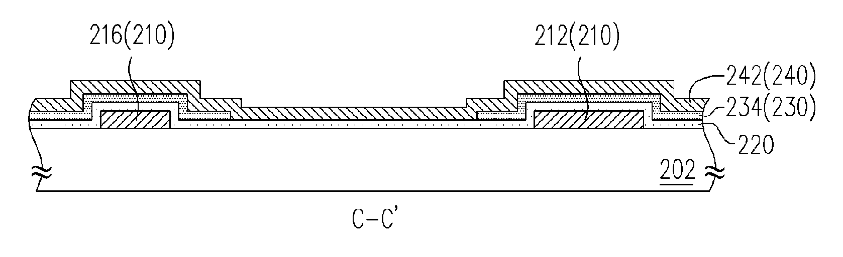
[0033] First, as shown in FIG. 2A, a substrate 202 is provided, wherein a plurality of pixel regions 202a are defined on the substrate 202 and a first metal layer 210 is formed on the substrate 202. Then, the first metal layer 210 is patterned to form a scan line 212 and a plurality of gates 214. In the embodiment, the substrate 202 is, for example, a glass substrate or a transparent substrate formed of other kind of material, and the first metal layer 210 is formed of material such as chromium (Cr), molybdenum (Mo), or wolfram (W).

[0034] Accordingly, when the present invention is patterning the first metal layer 210, a plurality of common lines 216 may be formed on the substrate 202, wherein the common lines 216 are parallel to the scan lines 212 and alternately disposed on the substrate with the scan...


PUM


Abstract

A thin film transistor array substrate and a manufacturing method thereof are provided. Wherein, scan lines and data lines are disposed on a substrate to define a plurality of pixel regions. Thin film transistors are disposed in the pixel regions correspondingly and driven by the scan lines and the data lines. Pixel electrodes are disposed in the pixel regions respectively and electrically connected to the corresponding thin film transistors. In addition, a gate insulating layer is disposed on the substrate to cover the scan lines and gates of the thin film transistors. A patterned leaning layer is disposed on the gate insulating layer and forms a plurality of non-continuous patterns under the data lines. The non-continuous patterns expose portions of the gate insulating layer under the data lines to which a portion of each data line can be directly attached.

Description

CROSS-REFERENCE TO RELATED APPLICATION [0001] This application claims the priority benefit of Taiwan application serial no. 94137108, filed on Oct. 24, 2005. All disclosure of the Taiwan application is incorporated herein by reference. BACKGROUND OF THE INVENTION [0002] 1. Field of Invention [0003] The present invention relates to an active device array substrate and a manufacturing method thereof, and particularly to a thin film transistor array substrate and a manufacturing method thereof. [0004] 2. Description of the Related Art [0005] Display is a communication interface between human and information. Nowadays, the flat display has become the trend of development in the display field. The flat panel display primarily includes: organic electroluminescence display (OLED), plasma display panel (PDP), and thin film transistor liquid crystal display (TFT-LCD). Wherein, the thin film transistor liquid crystal display is applied most generally. [0006] The thin film transistor liquid cr...

Claims


Application Information

Patent Timeline
Patent Type & Authority Applications(United States)
IPC IPC(8): H01L21/84H01L29/76H01L21/00
CPCG02F1/136204H01L27/124G02F1/136286
Inventor LIOU, MENG-CHICHEN, HSIAO-FEN
Owner CHUNGHWA PICTURE TUBES LTD
Why Eureka
Try Eureka