Checking wafer-level integrated designs for rule compliance

a technology of integrated circuit design and rule compliance, applied in the field of integrated circuit design, can solve problems such as voltage being applied to the circuit components, damage caused by plasma induced gate oxide, and charge buildup on circuit components

Active Publication Date: 2019-07-09
INT BUSINESS MASCH CORP
View PDF21 Cites 1 Cited by
  • Summary
  • Abstract
  • Description
  • Claims
  • Application Information

AI Technical Summary

Problems solved by technology

Plasma induced gate oxide damage is caused during the fabrication of an integrated circuit.
Various fabrication processes, in particular those that involve plasmas, can cause a charge buildup on circuit components.
This charge buildup results in a voltage being applied to the circuit components that is in excess of the tolerances of those devices.
In one specific example, the buildup of charge can cause a breakdown in the gate dielectric of a transistor, thereby damaging the transistor.
As the area of conductors increases, for example from component interconnects, the collected charge increases and the higher the likelihood of a breakdown.
Conversely, the greater the gate area, for example from multiple devices connected to the interconnect, the more the charge buildup will be spread out and the lower the likelihood of a breakdown.
These rules are referred to as “antenna rules,” and a violation of such rules is an “antenna violation.” While checking a circuit layout for rule compliance can adequately protect a circuit during fabrication, integrating multiple chips can dramatically increase the computational cost of performing full rule validation.

Method used


Image

  • Checking wafer-level integrated designs for rule compliance
  • Checking wafer-level integrated designs for rule compliance
  • Checking wafer-level integrated designs for rule compliance

Examples


Embodiment Construction

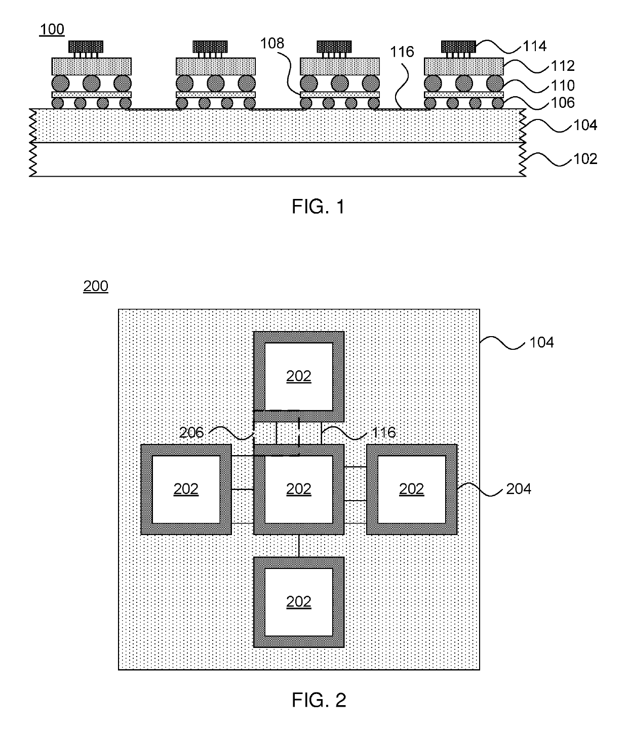
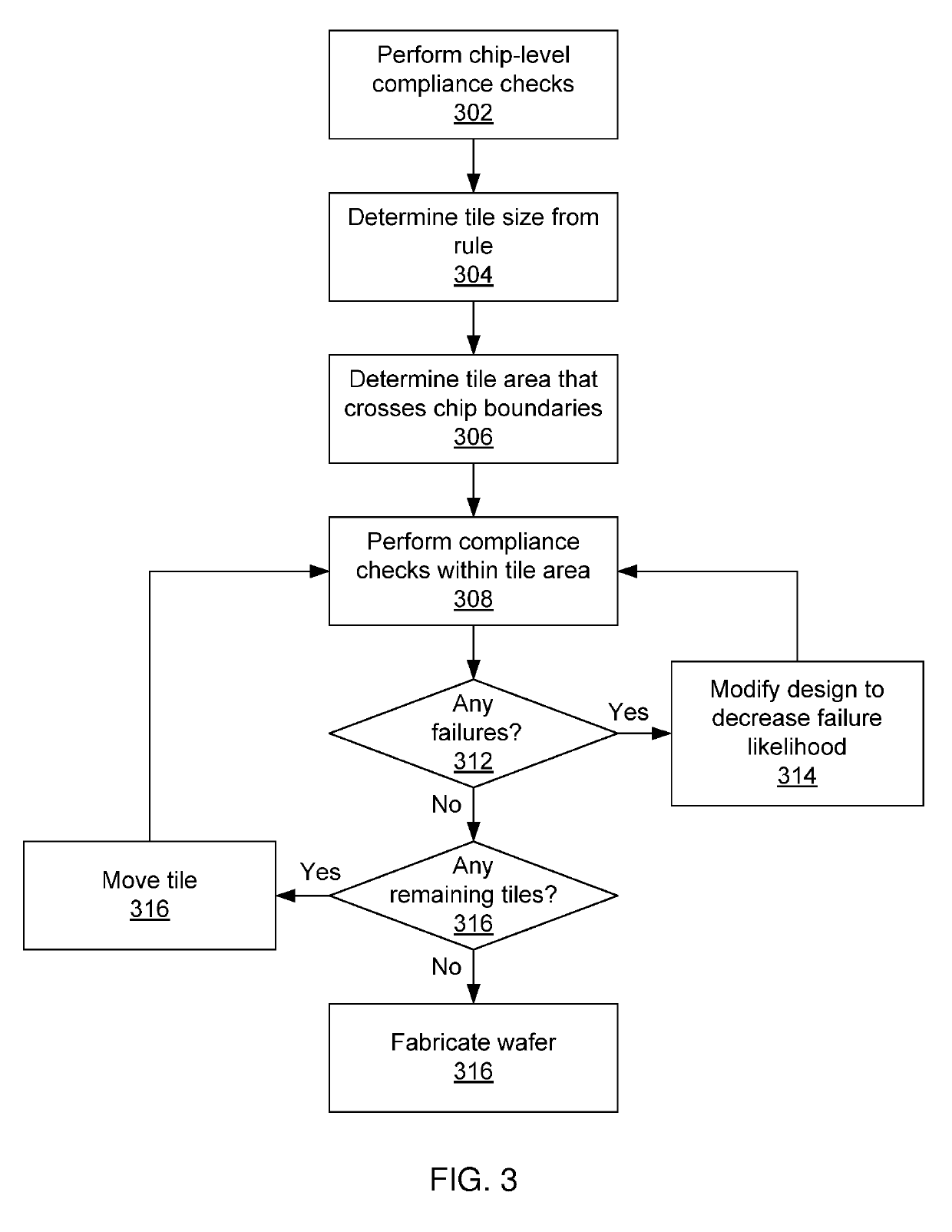
[0017]Embodiments of the present invention provide antenna rule compliance checking for wafer-level integration circuit layouts. Rather than combining multiple chips into one large layout for compliance checking, which would be time consuming and would likely also have many redundancies, the present embodiments test for rule compliance along the peripheries of chips. By using a tile of a fixed size that crosses chip boundaries, and by testing for compliance within the tile, rule compliance is evaluated for local rule compliance. The chips are checked separately, such that the interior of each chip need not be checked again when compliance across chip boundaries is checked.

[0018]Referring now to the drawings, in which like numerals represent the same or similar elements, and initially to FIG. 1, a cross-sectional view of an array of chips on a wafer 100 is shown. A wafer substrate is formed from, for example, an insulator layer 102 and a semiconductor layer 104. In one specific embod...


PUM


Abstract

Methods and systems for checking a wafer-level design for compliance with a rule include determining whether each chip layout out of multiple chip layouts complies internally with one or more layout design rules. A tile area is determined, having a size that is based on the one or more layout design rules, that crosses a boundary between adjacent chip layouts and that leaves at least a portion of each chip layout uncovered. It is determined whether portions of the plurality of chip layouts inside the tile area comply with the one or more layout design rules. The chip layouts are modified, if chip layout area within the tile area fails to comply with the design rule, to bring non-compliant periphery chip regions into compliance.

Description

BACKGROUND[0001]Technical Field[0002]The present invention relates to integrated circuit design and, more particularly, to checking for antenna rule compliance in integrated circuit designs that include multiple interconnected chips.[0003]Description of the Related Art[0004]Plasma induced gate oxide damage is caused during the fabrication of an integrated circuit. Various fabrication processes, in particular those that involve plasmas, can cause a charge buildup on circuit components. This charge buildup results in a voltage being applied to the circuit components that is in excess of the tolerances of those devices. In one specific example, the buildup of charge can cause a breakdown in the gate dielectric of a transistor, thereby damaging the transistor.[0005]Charge builds up in particular on conductors. As the area of conductors increases, for example from component interconnects, the collected charge increases and the higher the likelihood of a breakdown. Conversely, the greater...

Claims


Application Information

Patent Timeline
Patent Type & Authority Patents(United States)
IPC IPC(8): G06F17/50
CPCG06F17/5072G06F17/5081G06F30/398G06F30/392
Inventor HOOK, TERENCE B.WISSEL, LARRY
Owner INT BUSINESS MASCH CORP
Why Eureka
Try Eureka