Stacked package including exterior conductive element and a manufacturing method of the same

a technology of conductive elements and packaging, which is applied in the direction of semiconductor devices, semiconductor/solid-state device details, electrical apparatus, etc., can solve the problems of affecting the quality of stacked packages, the size of conventional stacked packages increases inevitably, and the bonding process takes a long time, so as to improve reliability, simplify the process of forming electrical connections, and increase the uph

Inactive Publication Date: 2019-07-16
POWERTECH TECHNOLOGY INC
View PDF12 Cites 1 Cited by
  • Summary
  • Abstract
  • Description
  • Claims
  • Application Information

AI Technical Summary

Benefits of technology

[0006]The main objective of the present invention is to provide a stacked package and a manufacturing method of the same that has higher UPH and better reliability. The stacked package has plurality of chip packages stacked on active surfaces of each other, a dielectric layer, a redistribution layer and a plurality of external terminals. Each chip package has an exterior conductive element formed on the active surface. Each exterior conductive element has a cut edge exposed on at least one of the lateral side of the chip package. The dielectric layer, the redistribution layer and the external terminals are formed in sequence on the lateral side with the exposed cut edges to form the electrical connection between the cut edges, the redistribution layer and the external terminals. Therefore, the process for forming the electrical connections is simplified to enhance the reliability and the UPH for manufacturing the stacked package.

Problems solved by technology

The intervals inevitably increase the size of the conventional stacked package.
Thus, the conventional stacked package with bonding wires does not easily achieve miniaturization.
In addition, the wire bonding process takes a lot of time since all of the wires for one conventional stacked package cannot be bonded simultaneously.
Therefore, the unit per hour (UPH) of the conventional stacked package manufactured by the wire bonding process is relatively low.
When the chips are connected to each other by the TSV and the micro bumps, the TSV increases stacked heights and processing complexity leading to larger package thickness and lower manufacturing yield.
When the dimension of the conventional stacked packages become larger and larger, the position shift of the micro bumps becomes greater and greater leading to poor packaging yield.

Method used


Image

  • Stacked package including exterior conductive element and a manufacturing method of the same
  • Stacked package including exterior conductive element and a manufacturing method of the same
  • Stacked package including exterior conductive element and a manufacturing method of the same

Examples


Embodiment Construction

[0026]With reference to the attached drawings, the present invention is described by means of the embodiment(s) below where the attached drawings are simplified for illustration purposes only to illustrate the structures or methods of the present invention by describing the relationships between the components and assembly in the present invention. Therefore, the components shown in the figures are not expressed with the actual numbers, actual shapes, actual dimensions, nor with the actual ratio. Some of the dimensions or dimension ratios have been enlarged or simplified to provide a better illustration. The actual numbers, actual shapes, or actual dimension ratios can be selectively designed and disposed and the detail component layouts may be more complicated.

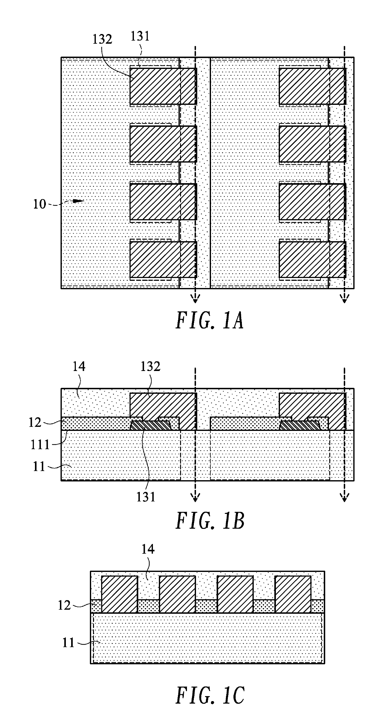
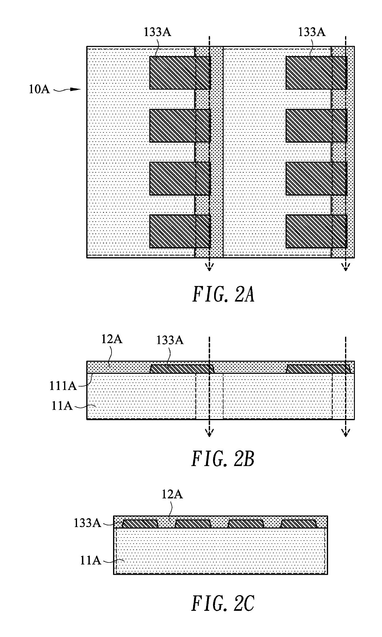
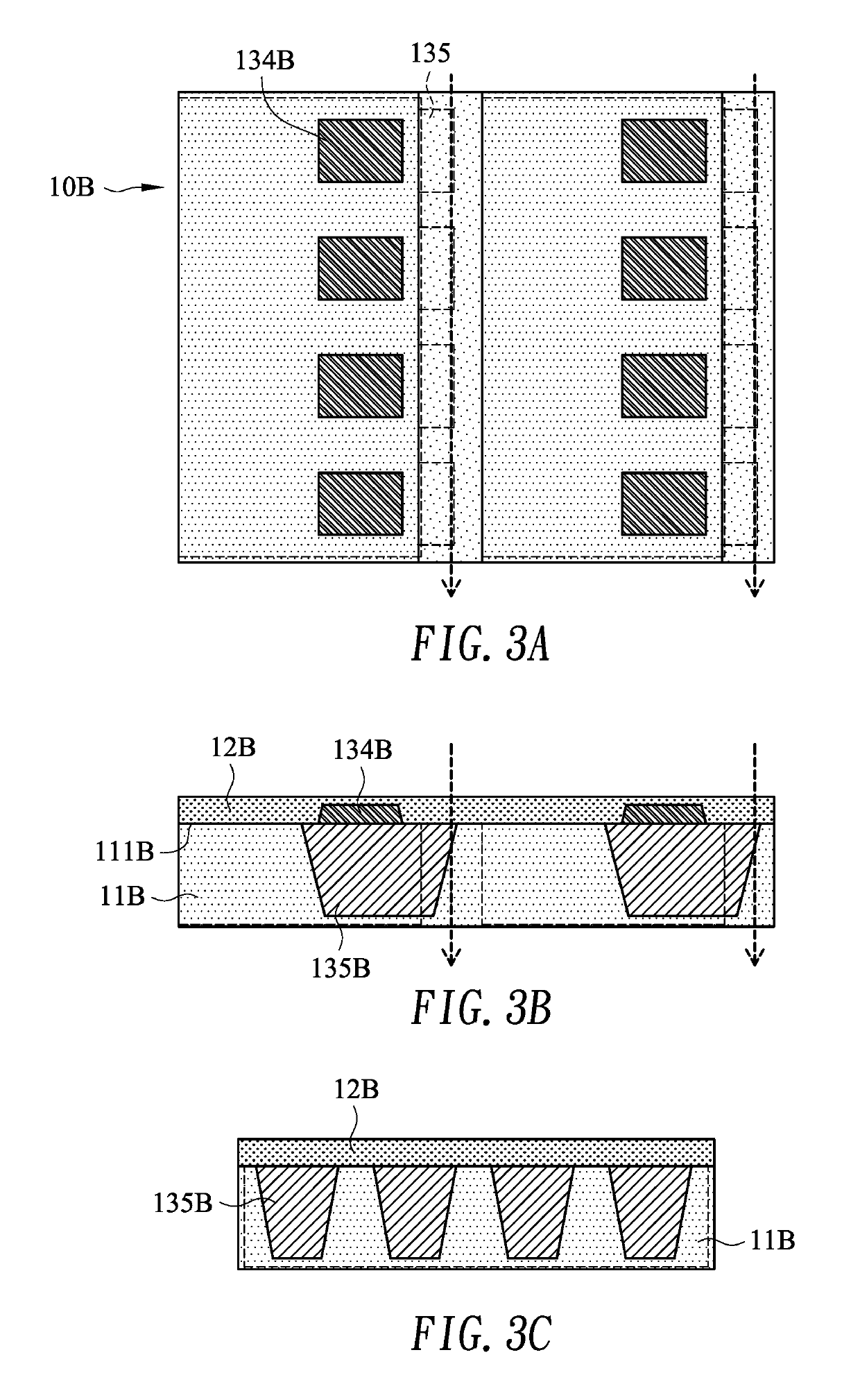
[0027]With reference to FIG. 15A, a stacked package 90 in accordance with the present invention comprises a plurality of chip packages 10. The chip package 10 has at least two lateral sides, a chip 11, a passivation layer 12 ...


PUM


Abstract

A stacked package has plurality of chip packages stacked on active surfaces of each other, a dielectric layer, a redistribution layer and a plurality of external terminals. Each chip package has an exterior conductive element formed on the active surface. Each exterior conductive element has a cut edge exposed on at least one of the lateral side of the chip package. The dielectric layer, the redistribution layer and the external terminals are formed in sequence on the lateral side with the exposed cut edges to form the electrical connection between the cut edges, the redistribution layer and the external terminals. Therefore, the process for forming the electrical connections is simplified to enhance the reliability and the UPH for manufacturing the stacked package.

Description

BACKGROUND OF THE INVENTION1. Field of the Invention[0001]The present invention relates to a semiconductor package, and in particular to a stacked package and a manufacturing method of the same.2. Description of the Prior Arts[0002]Stacking a plurality of chips has been implemented in various semiconductor packages to achieve miniaturization of component integration. The wire bonding method and the through silicon via (TSV) with micro bump are conventional ways to provide electrical interconnection between the stacked chips and the external terminals. However, the conventional ways have following disadvantages.[0003]When the chips are connected to the external terminals by wire bonding, the intervals between the bonding wires need to be preserved to avoid contacts between the adjacent bonding wires. The intervals inevitably increase the size of the conventional stacked package. Thus, the conventional stacked package with bonding wires does not easily achieve miniaturization. In addi...

Claims


Application Information

Patent Timeline
Patent Type & Authority Patents(United States)
IPC IPC(8): H01L25/065H01L21/56H01L23/00H01L21/768H01L25/00H01L23/48H01L21/78
CPCH01L25/0657H01L21/568H01L21/76898H01L21/78H01L23/481H01L24/02H01L24/05H01L24/13H01L24/96H01L25/50H01L21/561H01L2225/06582H01L2224/02372H01L2224/0401H01L2224/05024H01L2224/13026H01L2224/95001H01L2225/06513H01L2225/06544H01L2225/06555H01L24/24H01L24/20H01L2224/32145H01L2224/24145H01L2224/24135H01L2224/241H01L2224/211H01L2224/12105H01L2224/131H01L24/32H01L2224/73267H01L2224/92244H01L2224/96H01L24/19H01L24/82H01L24/25H01L2224/2518H01L2224/82005H01L24/92H01L2224/2105H01L2224/14181H01L24/14H01L2224/02371H01L2224/05548H01L2224/2919H01L24/29H01L2224/29294H01L2224/83101H01L2224/04105H01L2224/133H01L2224/13294H01L24/73H01L2224/221H01L23/5389H01L23/5384H01L23/49816H01L23/5385H01L23/3135H01L23/3128H01L2924/00012H01L2924/014H01L2224/19H01L2224/82H01L2224/11H01L2924/0665H01L2924/07802H01L2924/00014
Inventor CHEN, MING-CHIHHSU, HUNG-HSINLAN, YUAN-FUWANG, CHI-ANHSU, HSIEN-WEN
Owner POWERTECH TECHNOLOGY INC
Why Eureka
Try Eureka