Multi-location metrology

Active Publication Date: 2019-07-30
KLA TENCOR CORP
View PDF31 Cites 7 Cited by
  • Summary
  • Abstract
  • Description
  • Claims
  • Application Information

AI Technical Summary

Benefits of technology

[0011]The trained measurement models described herein receive optical measurement data directly as input and provide values of parameters of inte

Problems solved by technology

In addition, model-based metrology techniques include modeling errors induced by practical, computational limitations.
Hence, not all parameters are floated during computation, and this leads to errors in the estimates of parameter

Method used


Image

  • Multi-location metrology
  • Multi-location metrology
  • Multi-location metrology

Examples


Embodiment Construction

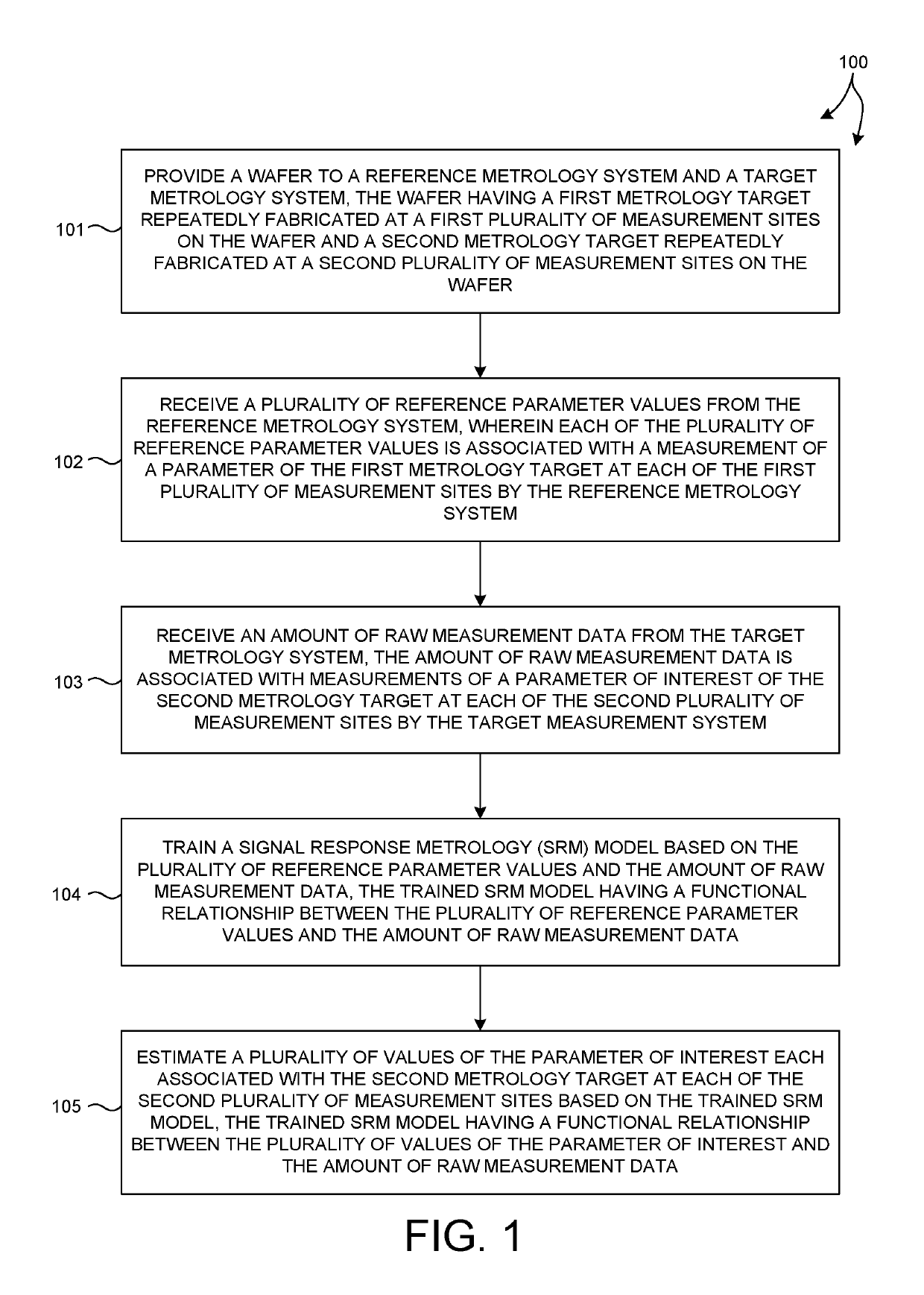
[0017]Reference will now be made in detail to background examples and some embodiments of the invention, examples of which are illustrated in the accompanying drawings.

[0018]Methods and systems for estimating values of parameters of interest of structures fabricated on a wafer with a signal response metrology (SRM) model trained based on reference measurement data collected from the same wafer are presented herein. The SRM model includes fewer errors than the reference measurements employed to train the SRM model.

[0019]Parameter values estimated by model-based metrology systems include errors from a number of sources. For example, the underlying measurement model may not properly model certain aspects of the structure or the system (e.g., random process variations). In addition, the values of many measurement model parameters are fixed during regression calculations. Hence, not all measurement model parameters are floated during regression. This introduces errors in the estimation o...


PUM


Abstract

Methods and systems for estimating values of parameters of interest of structures fabricated on a wafer with a signal response metrology (SRM) model trained based on reference measurement data collected from the same wafer are presented herein. In one aspect, the SRM model is an input-output model trained to establish a functional relationship between reference measurements of structures fabricated on the wafer to raw measurement data collected from the same wafer. The raw measurement data collected from the wafer is employed for training the SRM model and for performing measurements using the trained SRM model. In another aspect, the SRM model uses the entire set of raw measurement data collected from a number of measurement sites across the wafer for both training and subsequent measurement at each individual site. In a further aspect, the SRM model is trained and utilized to measure each parameter of interest individually.

Description

CROSS REFERENCE TO RELATED APPLICATION[0001]The present application for patent claims priority under 35 U.S.C. § 119 from U.S. provisional patent application Ser. No. 62 / 128,257, entitled “Multi-Location Metrology,” filed Mar. 4, 2015, the subject matter of which is incorporated herein by reference in its entirety.TECHNICAL FIELD[0002]The described embodiments relate to metrology systems and methods, and more particularly to methods and systems for improved measurement of structures fabricated in the semiconductor industry.BACKGROUND INFORMATION[0003]Semiconductor devices such as logic and memory devices are typically fabricated by a sequence of processing steps applied to a specimen. The various features and multiple structural levels of the semiconductor devices are formed by these processing steps. For example, lithography among others is one semiconductor fabrication process that involves generating a pattern on a semiconductor wafer. Additional examples of semiconductor fabrica...

Claims


Application Information

Patent Timeline
IPC IPC(8): G01B11/00G01N21/84H01L21/67
CPCG01N21/84H01L21/67253G01B11/00G01N21/8422G01N2201/12G01N2021/8416G01N2021/8883G01N21/95607G03F7/70616G03F7/705
Inventor PANDEV, STILIAN IVANOVLU, WEI
Owner KLA TENCOR CORP
Why Eureka
Try Eureka