

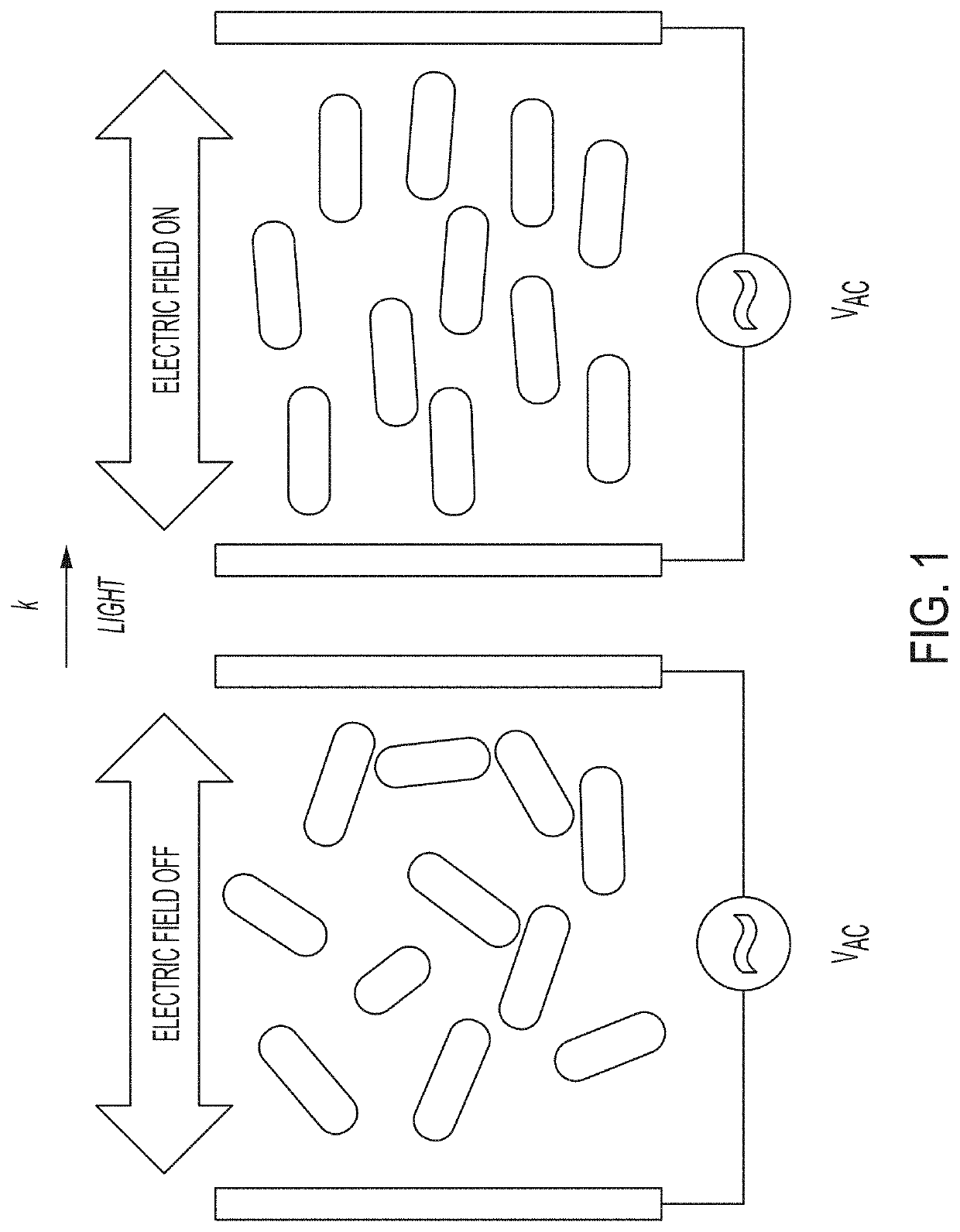
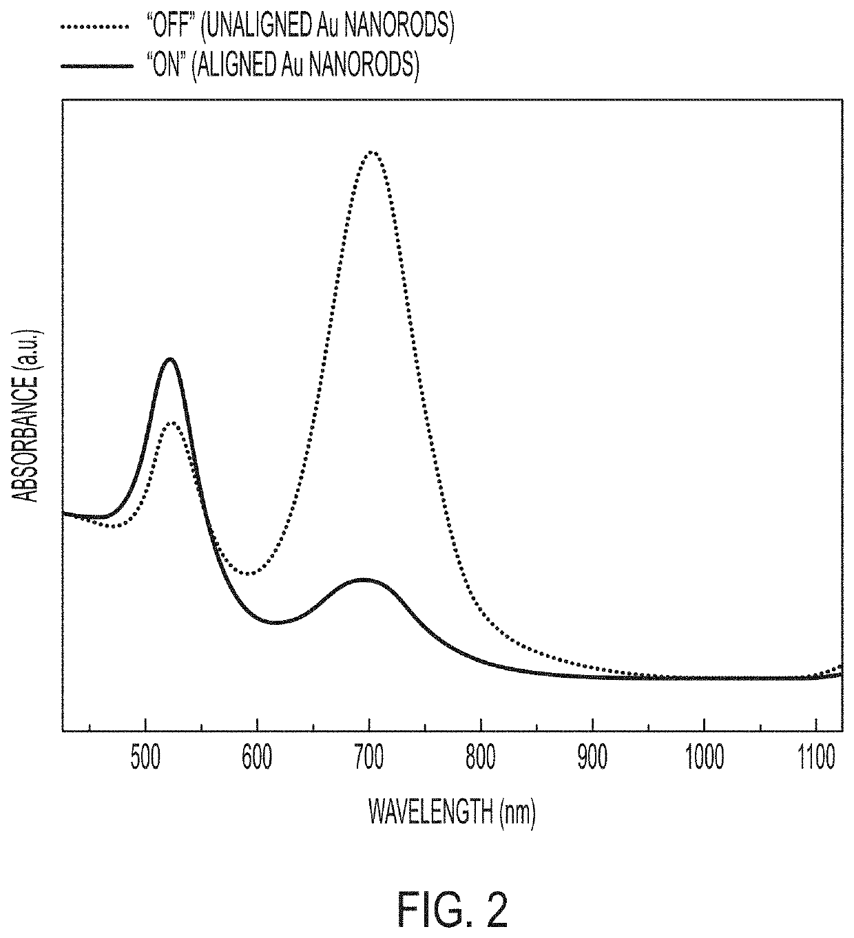
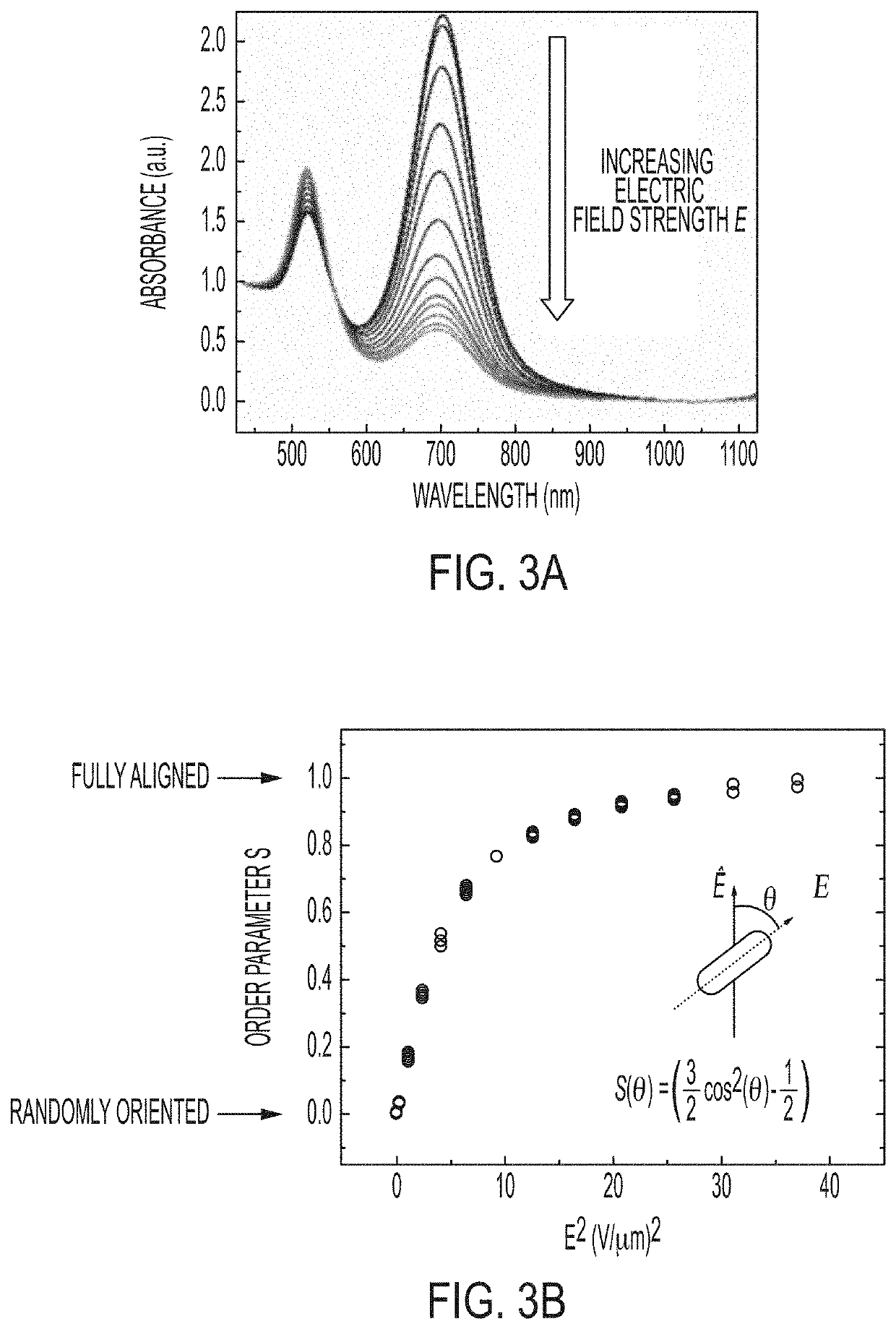
Plasmonic nanoparticles as pixels and sub-microsecond switches
a technology of plasmonic nanoparticles and sub-microsecond switches, which is applied in the direction of instrumentation, laser details, active medium shape and construction, etc., can solve the problems of limiting the application of real-time light modulation and limiting potential electro-optic applications for decades, and achieve the effect of controlling the chromaticity and/or luminance of perceived colors
- Summary
- Abstract
- Description
- Claims
- Application Information
AI Technical Summary
Benefits of technology
Problems solved by technology
Method used
Image

Examples
Embodiment Construction
Definitions
[0022]Before describing the present invention in detail, it is to be understood that the terminology used in the specification is for the purpose of describing particular embodiments, and is not necessarily intended to be limiting. Although many methods, structures and materials similar, modified, or equivalent to those described herein can be used in the practice of the present invention without undue experimentation, the preferred methods, structures and materials are described herein. In describing and claiming the present invention, the following terminology will be used in accordance with the definitions set out below.
[0023]As used herein, the singular forms “a”, “an,” and “the” do not preclude plural referents, unless the context clearly dictates otherwise.
[0024]As used herein, the term “and / or” includes any and all combinations of one or more of the associated listed items.
[0025]As used herein, the term “about” when used in conjunction with a stated numerical value...
PUM
| Property | Measurement | Unit |
|---|---|---|
| length | aaaaa | aaaaa |
| aspect ratio | aaaaa | aaaaa |
| electric field | aaaaa | aaaaa |
Abstract
Description
Claims
Application Information