Check patentability & draft patents in minutes with Patsnap Eureka AI!

Pressure sensor and manufacturing method thereof

a technology of pressure sensor and manufacturing method, which is applied in the field of pressure sensor, can solve problems such as difficulty in manufacturing diaphragms, and achieve the effects of reducing defect rate, high alignment precision, and optimizing the performance of pressure sensor

Active Publication Date: 2020-08-11
KOREA ELECTRONICS TECH INST
View PDF3 Cites 0 Cited by
  • Summary
  • Abstract
  • Description
  • Claims
  • Application Information

AI Technical Summary

Benefits of technology

[0005]Accordingly, the present invention has been made keeping in mind the above problems occurring in the related art, and an object of the present invention is to provide a pressure sensor using a silicon nanowire having a high piezoresistivity as a sensing element. Additionally, the present invention is intended to provide a pressure sensor having a structure in which stress due to deformation at a boundary of a diaphragm can be easily and reliably transferred to a silicon nanowire, and to provide a method of manufacturing the same.
[0016]In addition, the diaphragm region is formed by etching the upper substrate while using the silicon nanowire as an alignment reference position for the etching. Therefore, the silicon nanowire can be formed at the boundary of the diaphragm region. That is, since the silicon nanowire can be formed at a region where mechanical deformation is greatest, the performance of the pressure sensor can be maximized.
[0017]In addition, since the diaphragm region is defined in the upper substrate, the only requirement for the diaphragm recess is that the size of the diaphragm recess is larger than the size of the diaphragm region. Therefore, the diaphragm recess is formed, a high alignment precision with respect to the silicon nanowire is not required. This results in a decrease in defect rate when manufacturing pressure sensors.

Problems solved by technology

However, since the diaphragm is famed by bulk-etching the backside of a substrate, it is difficult to manufacture the diaphragm such that the boundary of the diaphragm is precisely aligned with the piezoresistive element.

Method used


Image

  • Pressure sensor and manufacturing method thereof
  • Pressure sensor and manufacturing method thereof
  • Pressure sensor and manufacturing method thereof

Examples


Embodiment Construction

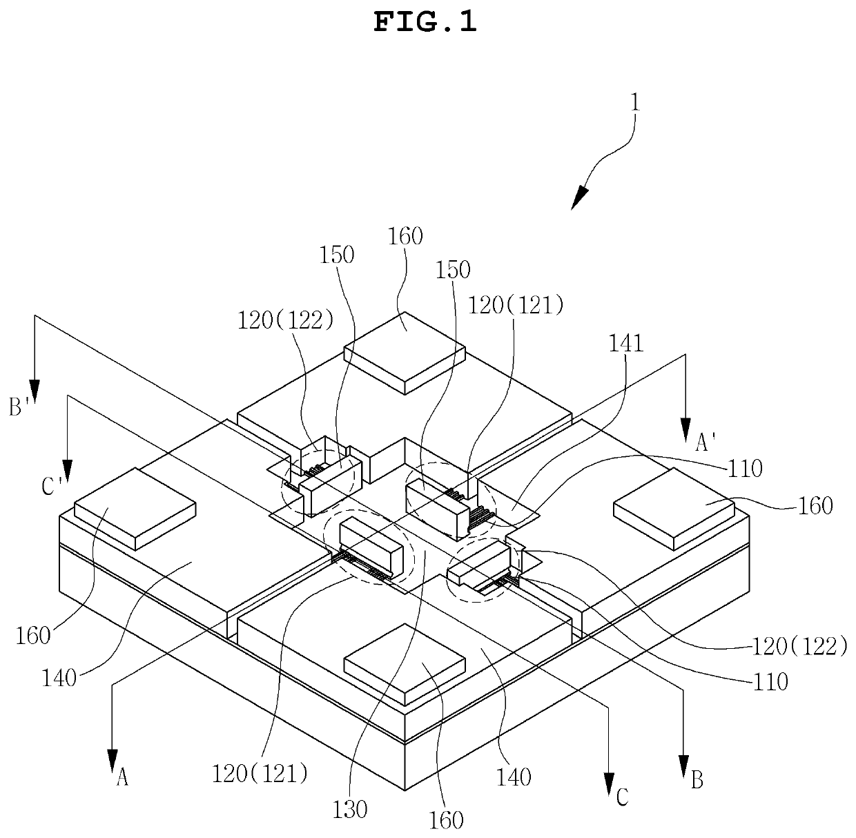
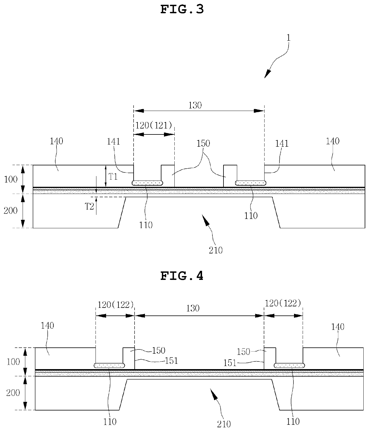
[0030]Reference now should be made to the drawings, in which the same reference numerals are used throughout the different drawings to designate the same or similar components.

[0031]The above and other objects, features and advantages of the present invention will be more clearly understood from the following detailed description taken in conjunction with the accompanying drawings. Reference now should be made to the drawings, in which the same reference numerals are used throughout the different drawings to designate the same or similar components. Further, it will be understood that, although the terms “one side”, “the other side”, “first,”“second,” etc. may be used herein to describe various elements, these elements should not be limited by these terms. Further, when it is determined that the detailed description of the known art related to the present invention might obscure the gist of the present invention, the detailed description thereof will be omitted.

[0032]Herein below, e...


PUM

PropertyMeasurementUnit
pressureaaaaaaaaaa
electrical resistanceaaaaaaaaaa
mechanical deformationaaaaaaaaaa

Abstract

Disclosed is a silicon nanowire pressure sensor including a lower substrate with a diaphragm recess in a lower surface thereof, an upper substrate having a first surface attached to an upper surface of the lower substrate, silicon nanowires formed on the first surface of the upper substrate, resistive portions exposed on a second surface of the upper substrate, and a diaphragm region formed by etching a center portion of the second surface of the upper substrate so as to be aligned with the resistive portions, in which the diaphragm recess is larger than the diaphragm region.

Description

CROSS REFERENCE TO RELATED APPLICATION(S)[0001]This application claims the benefit of Korean Patent Application No. 10-2017-0165992, filed Dec. 5, 2017, entitled Pressure Sensor and Manufacturing Method Thereof, which is hereby incorporated by reference in its entirety into this application.BACKGROUND OF THE INVENTION1. Technical Field[0002]The present invention relates to a pressure sensor and a method of manufacturing the same. More particularly, the present invention relates to a pressure sensor using a silicon nanowire as a piezoelectric element, the pressure sensor being configured such that mechanical deformation of a sensing film due to pressure applied thereto is transferred to a specific portion of a silicon nanowire piezoelectric element, and a method of manufacturing the same.2. Description of the Background Art[0003]In a conventional pressure sensor, a piezoresistive element is formed as a doped region formed through a doping process in a silicon substrate. Such a conven...

Claims


Application Information

Patent Timeline
Patent Type & Authority Patents(United States)
IPC IPC(8): H01L41/08H01L41/39H01L29/84H01L41/113H01L29/06G01L9/00H01L41/18
CPCH01L41/18H01L41/39H01L41/1132H01L29/0669H01L29/84G01L9/0055G01L9/0042H01L41/0805G01H9/00G01L7/08H10N30/1051H10N30/85H10N30/093H10N30/302
Inventor JUNG, SUK WONCHO, NAM KYU
Owner KOREA ELECTRONICS TECH INST
Features
  • R&D
  • Intellectual Property
  • Life Sciences
  • Materials
  • Tech Scout
  • Unparalleled Data Quality
  • Higher Quality Content
  • 60% Fewer Hallucinations
Learn More