Electronic component

a technology of electronic components and components, applied in piezoelectric/electrostrictive/magnetostrictive devices, piezoelectric/electrostrictive device manufacture/assembly, electrical apparatus, etc., can solve the problems of affecting the heat dissipation efficiency of the components, the likely accumulation of heat inside, and the likely deformation of frequency temperature characteristics, etc., to achieve efficient improvement of heat dissipation properties

Active Publication Date: 2020-10-20
MURATA MFG CO LTD
View PDF15 Cites 0 Cited by
  • Summary
  • Abstract
  • Description
  • Claims
  • Application Information

AI Technical Summary

Benefits of technology

[0007]Preferred embodiments of the present invention provide electronic components that achieve improved heat dissipation properties and significantly reduce or prevent deformation of a cover at the time of forming a mold resin layer.
[0015]In still another electronic component according to a preferred embodiment of the present invention, a height of an uppermost portion of the cover is lower than a height of an upper end of the bonding member.
[0016]In another electronic component according to a preferred embodiment of the present invention, the height of the uppermost portion of the cover is higher than the height of the upper end of the bonding member.
[0019]According to electronic components of preferred embodiments of the present invention, the deformation of the cover is unlikely to occur even if sealing with resin is carried out. In addition, heat dissipation properties thereof are efficiently improved.

Problems solved by technology

With such structure, heat is likely to accumulate inside thereof.
As such, there is a problem that frequency temperature characteristics are likely to be degraded.
In addition, due to inflow-pressure of the resin at a time of molding, there is a risk that the cover, the cover unit, or the protective resin portion described in Japanese Unexamined Patent Application Publication No. 2007-19943 is so deformed as to project toward the piezoelectric substrate side in a center region of the hollow portion.
In the case where an amount of deformation becomes large, there is a risk of the cover, the cover unit, or the like making contact with the IDT electrode or the like.

Method used


Image

  • Electronic component
  • Electronic component
  • Electronic component

Examples


Embodiment Construction

[0033]Hereinafter, the present invention will be clarified through the description of specific preferred embodiments of the present invention with reference to the drawings.

[0034]It is to be noted that the preferred embodiments described in the present specification are merely examples and replacement or combination of the configurations can be partially made between different preferred embodiments.

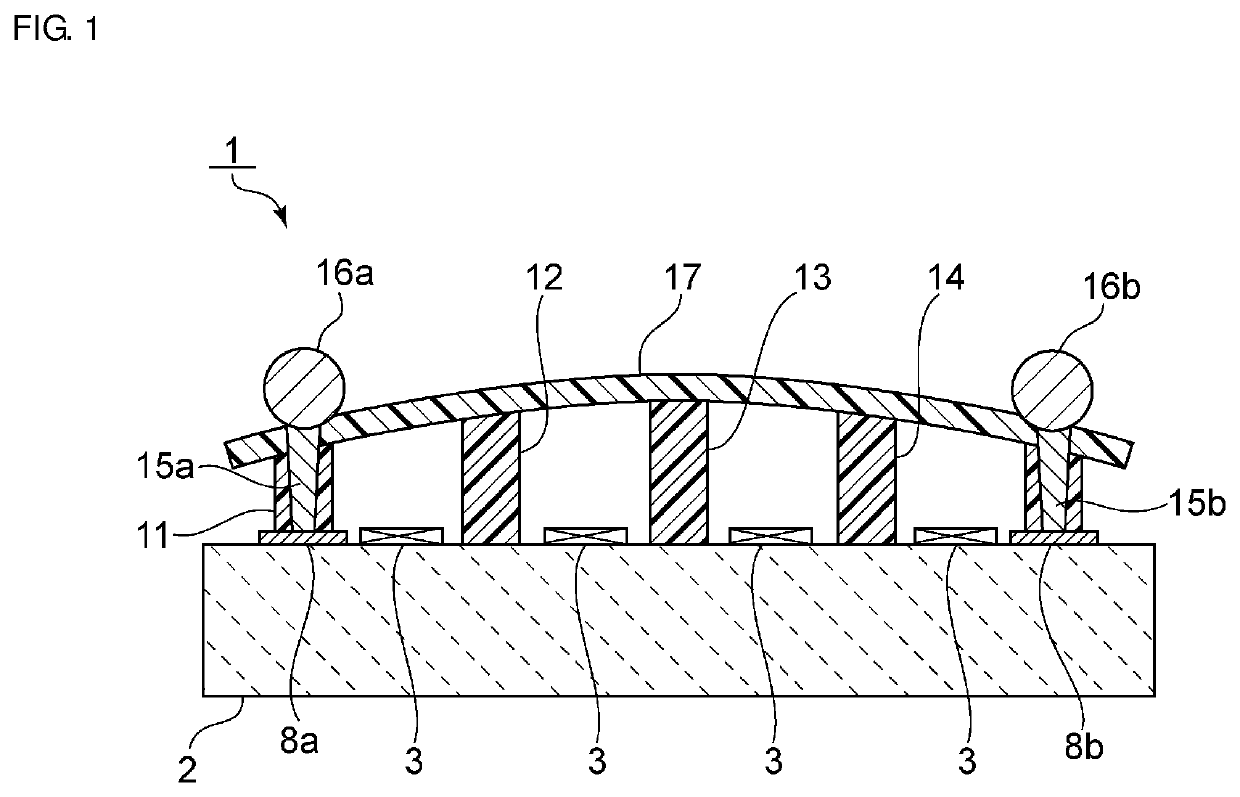
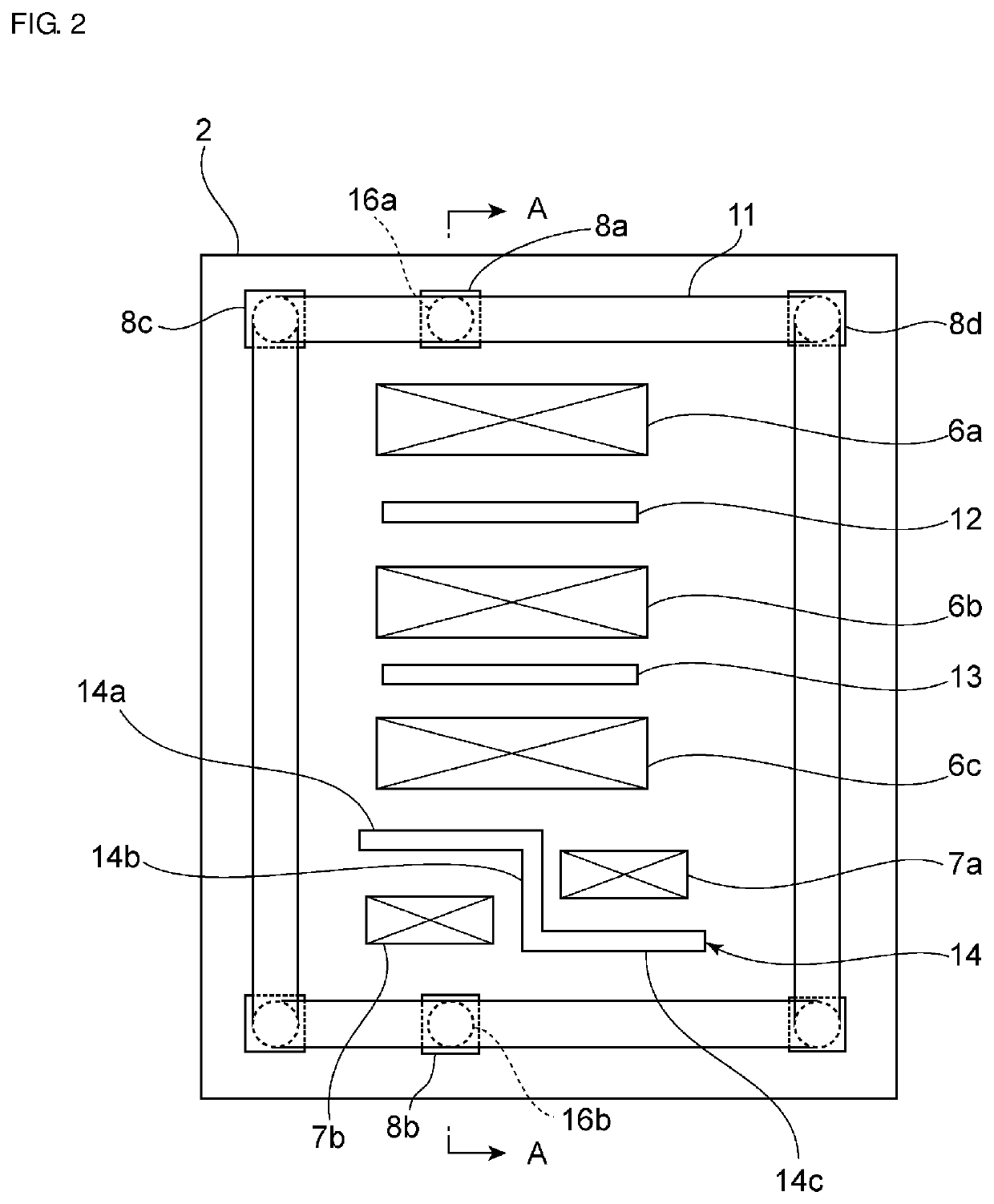
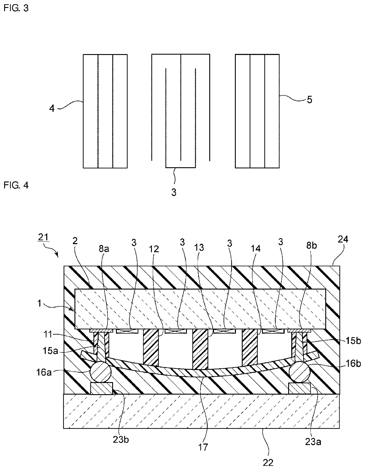
[0035]FIG. 1 is a cross-sectional side view of an electronic component according to a first preferred embodiment of the present invention, and FIG. 2 is a plan view illustrating a state where a cover to be explained later is removed in the electronic component according to the first preferred embodiment.

[0036]Note that FIG. 1 is a cross-sectional view of a portion corresponding to a portion taken along an A-A line in FIG. 2.

[0037]As shown in FIG. 1, an electronic component 1 includes a piezoelectric substrate 2. The piezoelectric substrate 2 preferably is formed of a 42° Y cut X SAW propa...


PUM


Abstract

In an electronic component, electrodes defining functional portions are provided on a piezoelectric substrate. In order to define a hollow portion which the functional portions face, there are provided a first support with a frame shape, and second supports on the piezoelectric substrate in an inner side region surrounded by the first support. A cover is laminated on the first support as well as on the second supports to define the hollow portion. A height of each of the second supports is higher than a height of the first support.

Description

CROSS REFERENCE TO RELATED APPLICATIONS[0001]This application claims the benefit of priority to Japanese Patent Application No. 2015-066207 filed on Mar. 27, 2015 and is a Continuation application of PCT Application No. PCT / JP2016 / 059615 filed on Mar. 25, 2016. The entire contents of each application are hereby incorporated herein by reference.BACKGROUND OF THE INVENTION1. Field of the Invention[0002]The present invention relates to electronic components such as surface acoustic wave devices and the like, for example.2. Description of the Related Art[0003]A package structure including a hollow portion is employed for surface acoustic wave devices and the like. For example, in an electronic component package disclosed in Japanese Unexamined Patent Application Publication No. 2007-129002, a plurality of electronic component elements are disposed on a component substrate. Partition walls for partitioning the plurality of electronic component elements from each other are provided. On th...

Claims


Application Information

Patent Timeline
Patent Type & Authority Patents(United States)
IPC IPC(8): H03H9/25H01L41/053H03H9/145H03H9/10H01L41/22
CPCH03H9/1071H03H9/145H01L41/053H03H9/25H01L41/22H03H9/125H10N30/88H10N30/01
Inventor TAKESHITA, TORU
Owner MURATA MFG CO LTD
Why Eureka
Try Eureka