Multilayer resin substrate and electronic component

a multi-layer resin and electronic component technology, applied in the direction of printed circuit manufacturing, printed circuit stress/warp reduction, printed circuit aspects, etc., can solve the problems of deformation or distortion, deformation or deformation in the stacking direction and the deformation or deformation of the multi-layer resin substrate to become more significant, so as to reduce or prevent delamination and deformation, reduce or prevent deformation and distortion of the multi-layer resin substra

Pending Publication Date: 2022-02-10
MURATA MFG CO LTD
View PDF0 Cites 0 Cited by
  • Summary
  • Abstract
  • Description
  • Claims
  • Application Information

AI Technical Summary

Benefits of technology

[0018]According to preferred embodiments of the present invention, multilayer resin substrates and electronic components that are each able to significantly reduce or prevent delamination and deformation due to gas pressure produced in an insulating resin base material layer and significantly reduce or prevent deformation and distortion of the multilayer resin substrate due to expansion and contraction are provided.

Problems solved by technology

For example, in a case in which the conductor pattern is metal foil, such as copper foil, the conductor pattern expands and contracts according to a linear expansion coefficient, and then the insulating resin base material layers change compositional properties around the glass transition temperature, which results in expansion and contraction.
As a result, the multilayer resin substrate is prone to deformation in the stacking direction, such as warping or twisting, or distortion in an in-plane direction, during heating.
In a structure of the multilayer resin substrate disclosed in Japanese Unexamined Patent Application Publication No. 2005-136347, when the gas vent holes are provided near an outer end or an end portion of the multilayer resin substrate and the multilayer resin substrate receives heat, stress applied to an interface between the conductor pattern and the insulating resin base material layer near the outer end or the end portion of the multilayer resin substrate may become uneven, which may cause the deformation or the distortion to become more significant.

Method used


Image

  • Multilayer resin substrate and electronic component
  • Multilayer resin substrate and electronic component
  • Multilayer resin substrate and electronic component

Examples


first preferred embodiment

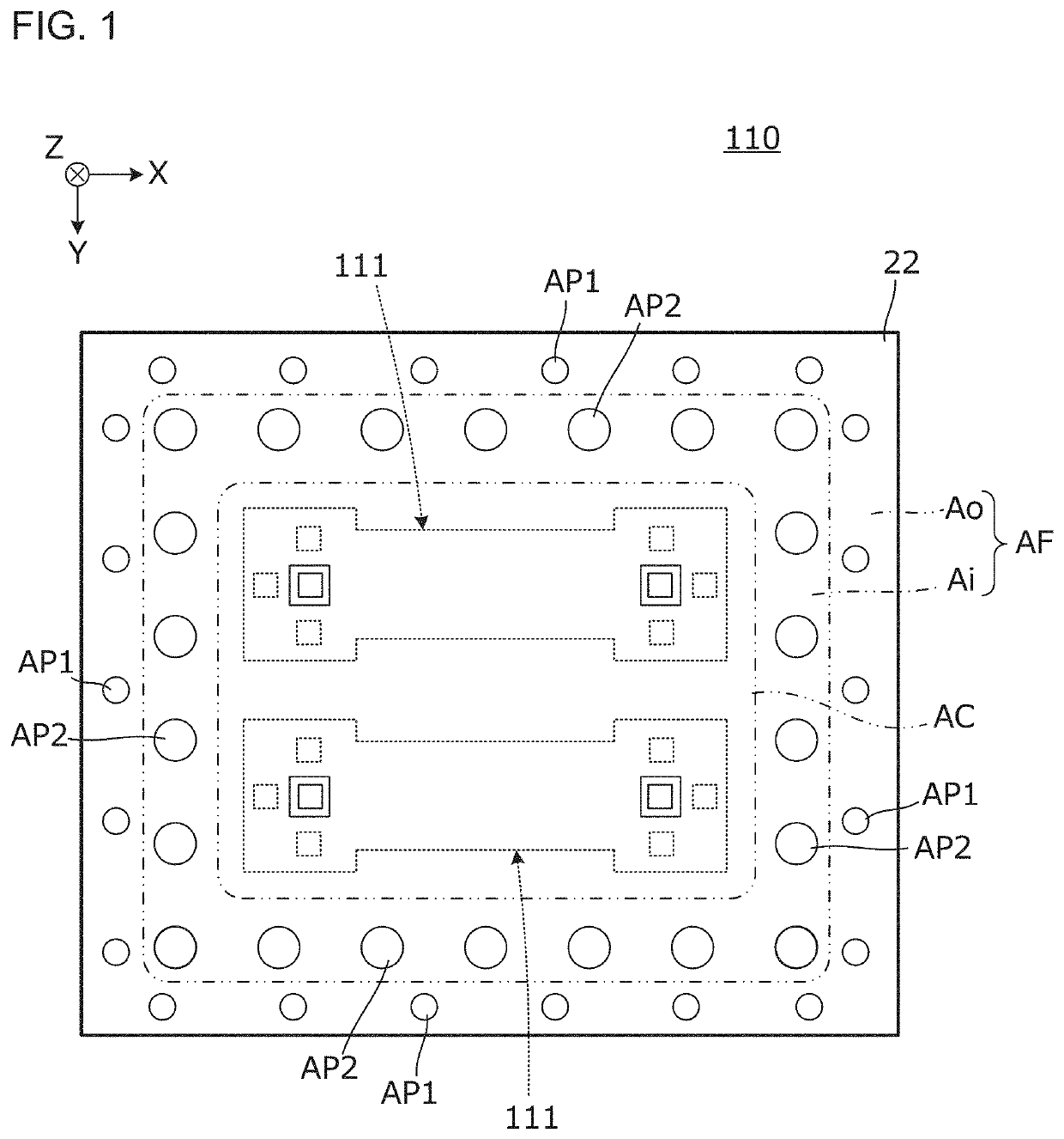
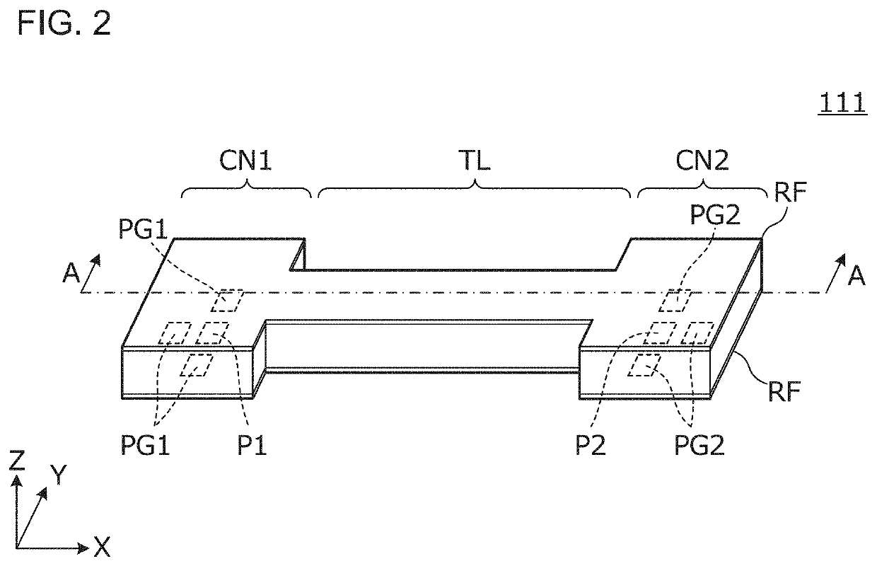
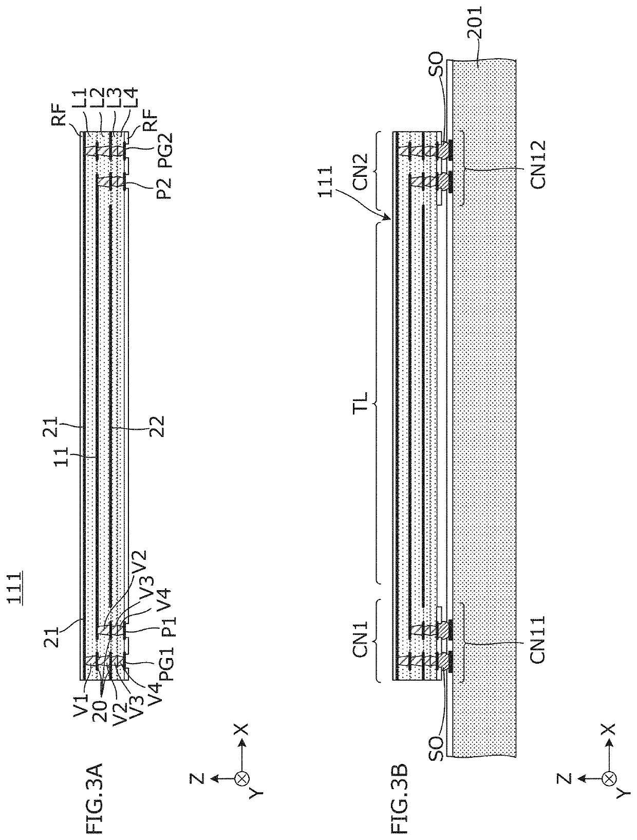
[0032]FIG. 1 is a plan view of a multilayer resin substrate 110 according to a first preferred embodiment of the present invention. The multilayer resin substrate 110 is a collective substrate including an electronic component configuration region AC that defines a plurality of electronic components (two electronic components in this example) 111 and a frame region AF that supports the electronic component configuration region AC. Accordingly, the electronic component 111 corresponds to a “child board” when the collective substrate is referred to as a “parent board.”FIG. 2 is a perspective view of the electronic component 111 separated from the multilayer resin substrate 110. Herein, the “electronic component” is a broad term that refers to an electronic component used not only for an active element or a passive element but for an electronic circuit device.

[0033]The multilayer resin substrate 110 includes a plurality of insulating resin base material layers, and a plurality of condu...

second preferred embodiment

[0053]A second preferred embodiment of the present invention provides an example of an electronic component including a multilayer resin substrate.

[0054]FIG. 5 is a perspective view showing a mounting structure of an electronic component 112 according to the second preferred embodiment of the present invention. FIG. 6 is a vertical cross-sectional view along a line X-X in FIG. 5. The electronic component 112 according to the present preferred embodiment is surface-mounted on the circuit board 201 and defines and functions as a signal transmission line.

[0055]As shown in FIG. 5 and FIG. 6, the electronic component 112 according to the present preferred embodiment includes a stacked body including a plurality of insulating resin base material layers, a transmission line portion TL provided on the stacked body, a first connection portion CN1 connected to a first portion of the transmission line portion TL, and a second connection portion CN2 connected to a second portion of the transmis...

third preferred embodiment

[0071]A third preferred embodiment of the present invention shows a configuration of an opening for degassing being different from the opening in the examples described above.

[0072]FIG. 10 is a partial plan view of a multilayer resin substrate according to the third preferred embodiment of the present invention. While, in the example shown in FIG. 1, the plurality of openings AP1 for degassing are provided in the outer peripheral portion Ao of the ground conductor 22, and the plurality of openings AP2 for degassing are provided in the inner peripheral portion Ai, in the third preferred embodiment, a plurality of openings AP are provided continuously from the outer peripheral portion Ao to the inner peripheral portion Ai. Other configurations are the same or substantially the same as the configurations of the multilayer resin substrate 110 described in the first preferred embodiment.

[0073]In the present example, the openings AP have a trapezoidal shape tapering in the outer periphera...


PUM

PropertyMeasurementUnit
areaaaaaaaaaaa
sizeaaaaaaaaaa
widthaaaaaaaaaa

Abstract

A multilayer resin substrate includes insulating resin base material layers, and conductor patterns on at least one of the insulating resin base material layers. The conductor patterns include a ground conductor on a main surface of the insulating resin base material layers and extend into a frame shape or a planar shape, and the ground conductor includes openings. An aperture ratio of the openings in an outer peripheral portion of the ground conductor is less than an aperture ratio of the openings in an inner peripheral portion of the ground conductor.

Description

CROSS REFERENCE TO RELATED APPLICATIONS[0001]This application claims the benefit of priority to Japanese Patent Application No. 2019-092473 filed on May 15, 2019 and is a Continuation Application of PCT Application No. PCT / JP2020 / 018944 filed on May 12, 2020. The entire contents of each application are hereby incorporated herein by reference.BACKGROUND OF THE INVENTION1. Field of the Invention[0002]The present invention relates to a multilayer resin substrate that includes a plurality of insulating resin base material layers and a plurality of conductor patterns provided on the plurality of insulating resin base material layers, and an electronic component that includes a signal line and a ground conductor.2. Description of the Related Art[0003]Japanese Unexamined Patent Application Publication No. 2005-136347 discloses a multilayer substrate made of a thermoplastic resin, the multilayer substrate including a conductor pattern configured by a wiring portion as a circuit portion, a l...

Claims


Application Information

Patent Timeline
Patent Type & Authority Applications(United States)
IPC IPC(8): H05K1/02H05K1/03H05K1/14
CPCH05K1/0298H05K1/141H05K1/032H05K1/0271H05K2201/09136H05K2201/068H05K1/0225H05K2201/0969H05K2201/0141H05K3/368
Inventor SATO, TAKAKOMAEGAWA, HIROKI
Owner MURATA MFG CO LTD
Why Eureka
Try Eureka