
Light guide plate stamp and method of manufacturing the same

a technology of light guide plate and stamp, which is applied in the field of stamps, can solve the problems of fine optical pattern deformation, deformation or other damage of stamp, etc., and achieve the effects of reducing or preventing deterioration of image quality, reducing strength of resulting stamp, and increasing strength

Inactive Publication Date: 2013-12-31
SAMSUNG DISPLAY CO LTD
View PDF13 Cites 2 Cited by
  • Summary
  • Abstract
  • Description
  • Claims
  • Application Information

AI Technical Summary

Benefits of technology

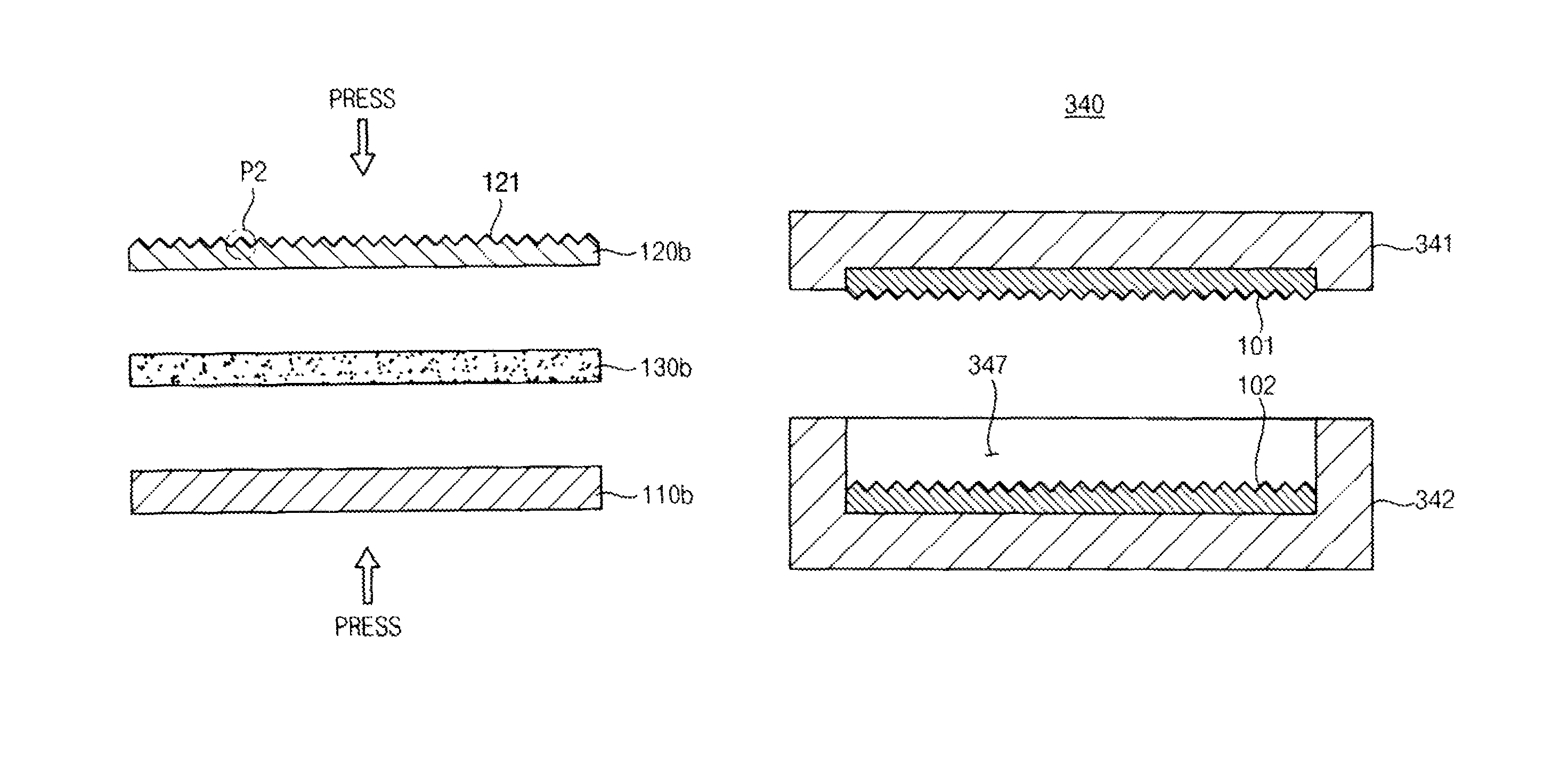
[0009]Example embodiments of the present invention provide a stamp that may reduce or prevent deformation in the process of manufacturing a light guide plate.
[0023]According to the example embodiments of the present invention, a metal supporting layer having a higher strength is combined with a pattern forming layer so that the strength of a resulting stamp may be improved. Thus, deformation of the stamp in the process of manufacturing a light guide plate and deterioration of image quality may be reduced or prevented, thereby increasing productivity of the light guide plate. Furthermore, the adhesive layer has a relatively low thermal conductivity. This improves transcription of an optical pattern.

Problems solved by technology

This high heat can result in deformation or other damage to the stamp.
Furthermore, damage or deformation of the stamp may also cause deformation of the fine optical pattern.

Method used


Image

  • Light guide plate stamp and method of manufacturing the same
  • Light guide plate stamp and method of manufacturing the same
  • Light guide plate stamp and method of manufacturing the same

Examples


Embodiment Construction

[0030]Hereinafter, the present invention will be explained in detail with reference to the accompanying drawings.

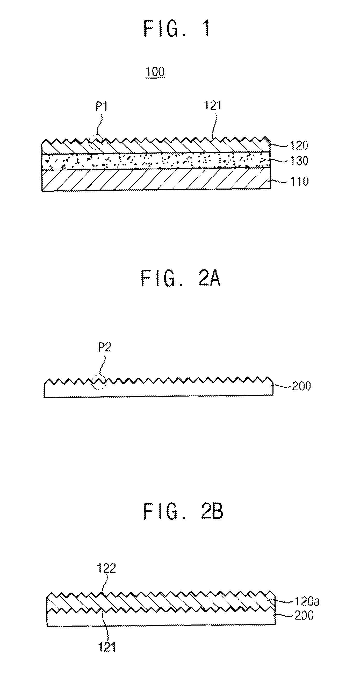
[0031]FIG. 1 is a cross-section view of a stamp according to an example embodiment of the present invention.

[0032]Referring to FIG. 1, stamp 100 includes a metal supporting layer 110, a pattern forming layer 120 and an adhesive layer 130.

[0033]The metal supporting layer 110 corresponds to a lowermost layer of the stamp 100, and has a first thermal conductivity. The metal supporting layer 110 is included in the stamp 100, and a higher strength than the pattern forming layer 120 so as to compensate for a low strength of the pattern forming layer 120 and to enhance mechanical strength of the stamp 100. The metal supporting layer 110 preferably has a dense structure and a high stiffness, and is easily processed to have a specular surface. Examples of a material that may be used for the metal supporting layer 110 may include a stainless steel such as SUS32.

[0034]The pattern fo...


PUM

PropertyMeasurementUnit
thermal conductivityaaaaaaaaaa
adhesiveaaaaaaaaaa
thicknessaaaaaaaaaa

Abstract

A stamp includes a metal supporting layer, a pattern forming layer and an adhesive layer. The metal supporting layer has a first thermal conductivity. The pattern forming layer is disposed on the metal supporting layer and has a surface with a molding pattern formed thereon. The adhesive layer is disposed between the metal supporting layer and the pattern forming layer to couple the pattern forming layer to the metal supporting layer, and has a second thermal conductivity lower than the first thermal conductivity. Thus, strength of the stamp may be improved, and deformation of the stamp during the process of manufacturing a light guide plate may be reduced or prevented.

Description

PRIORITY STATEMENT[0001]This application claims priority under 35 U.S.C. §119 to Korean Patent Application No. 2011-0033027, filed on Apr. 11, 2011 in the Korean Intellectual Property Office (KIPO), the contents of which are herein incorporated by reference in their entirety.BACKGROUND OF THE INVENTION[0002]1. Field of the Invention[0003]Example embodiments of the present invention relate to stamps for conducting stamping operations, as well as their methods of manufacture. More particularly, example embodiments of the present invention relate to a stamp that may be used for manufacturing a light guide plate that is to be used in flat panel displays, as well as a method of manufacturing the stamp.[0004]2. Description of the Related Art[0005]A liquid crystal display device is often characterized by small thickness, light weight and low power consumption. Accordingly, liquid crystal display devices have found widespread acceptance as monitors, notebook computers, mobile phones, and th...

Claims


Application Information

Patent Timeline
Patent Type & Authority Patents(United States)
IPC IPC(8): B29D7/00F21V7/04B29C45/34
CPCB21D47/04G02B6/00G02F1/13G02F1/1336G02F1/133611
Inventor RYU, HO-HANKIM, TAE-SEOKHONG, SEUNG-PYOLEE, SEUNG-YEOP
Owner SAMSUNG DISPLAY CO LTD
Learn More