

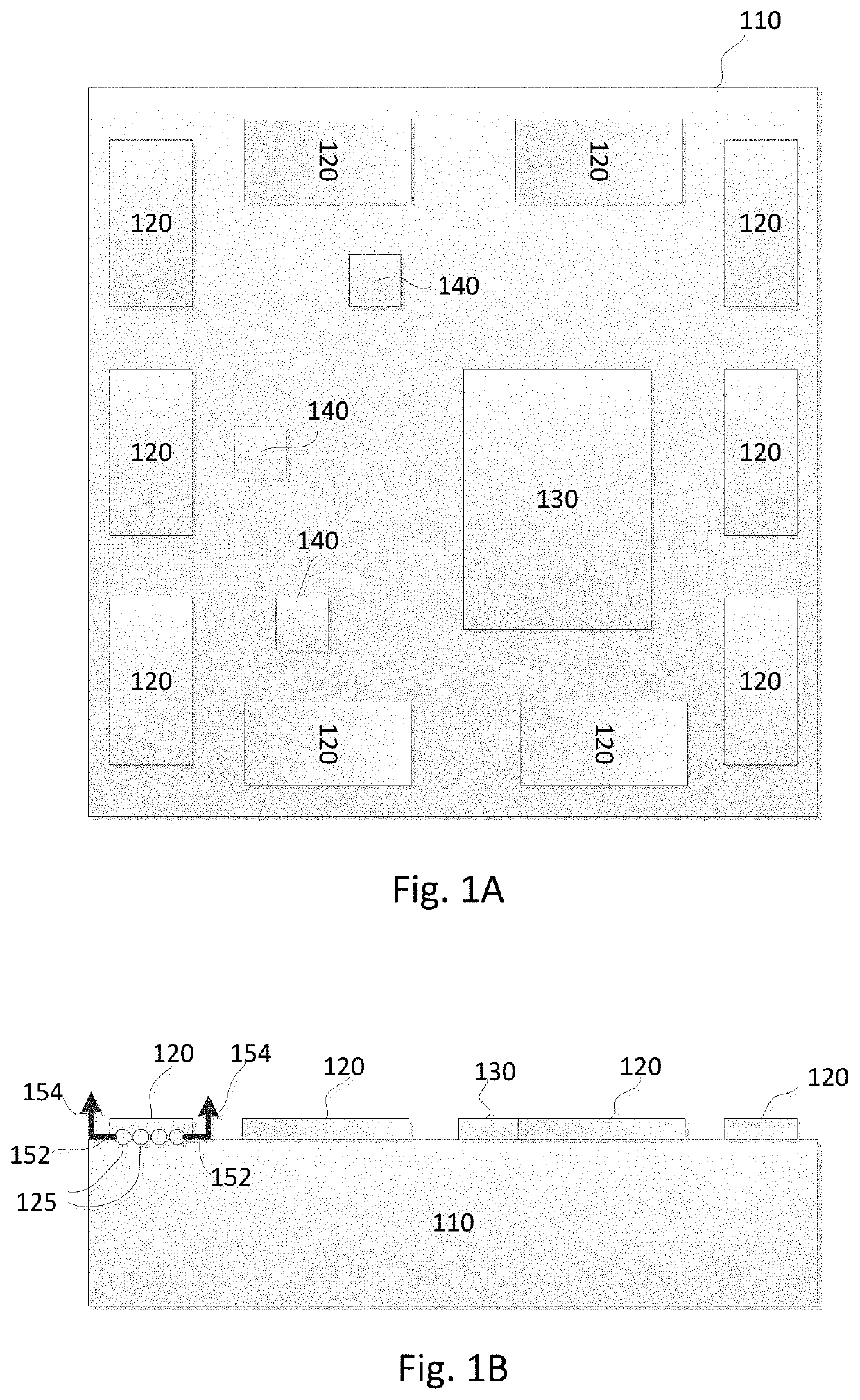
Hard IP blocks with physically bidirectional passageways
a bidirectional passageway and hard ip technology, applied in the field of hard ip blocks with bidirectional passageways, can solve the problems of gated computation, limited speed, inefficient second die, etc., and achieve the effect of not affecting transmitted signals
- Summary
- Abstract
- Description
- Claims
- Application Information
AI Technical Summary
Benefits of technology
Problems solved by technology
Method used
Image

Examples
Embodiment Construction
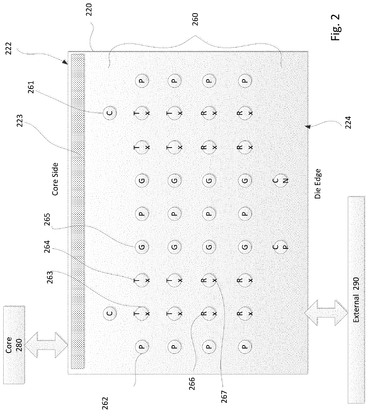
[0021]FIG. 2 illustrates a top view of an example configuration of a hard IP block, particularly a SerDes chip 220, including a plurality of surface interconnects 260. The surface interconnects 260 may be bumps, pads, or any other type of interconnect. Such interconnects include core power 261, power 262, ground 265, transmit pairs 263-264, receive pairs 266-267, positive and negative clocks, etc. A first side 222 of the chip 220 is referred to as a “core side” and is used for communicating with a core 280. As shown, the core side includes dense interconnects 223. A second side 224 is a die edge 224, and faces a periphery of the die hosting the SerDes block 220. The second side 224 may include much fewer interconnects than the core side 222, and maybe used to interface with external devices 290. In this regard, the SerDes chip 220 is able to take more highly-parallel, low-speed, low-voltage signals from the core side 222, serialize the received signals together, send the serialized ...
PUM
 Abstract
Description
Claims
Application Information