Output signal generation circuit
The output signal generation circuit addresses the challenge of managing multiple signals in control devices by superimposing information on a pulse signal with a minimum pulse width, enabling efficient transmission and operation of multiple functional units with fewer signal lines and terminals.
- Summary
- Abstract
- Description
- Claims
- Application Information
AI Technical Summary
Benefits of technology
Problems solved by technology
Method used
Image

Examples
embodiment 1
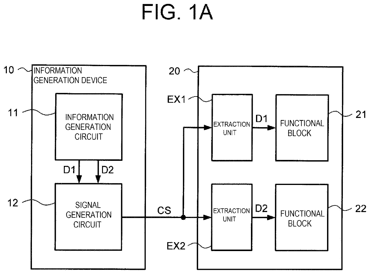
[0019]FIG. 1A is a block diagram showing a configuration of an information generation device 10 according to Embodiment 1, and a functional unit 20 connected to the information generation device 10. The information generation device 10 constitutes a microcontroller, for example. The functional unit 20 includes a plurality (two in the present embodiment) of functional blocks 21 and 22. The functional block 21 is a light-emitting element array for a display panel, and the functional block 22 is a speaker, for example. The configuration of the functional blocks 21 and 22 is not limited thereto. The functional blocks 21 and 22 simply need be a circuit block such as a motor, a heater, or a communication device that executes various functions by being driven by the information generation device 10.
[0020]The information generation device 10 is configured to perform various processes by acquiring information from input devices such as sensors, counters, and buttons (not shown), for example,...
embodiment 2
[0043]FIG. 4A is a block diagram showing a configuration of an information generation device 30 according to Embodiment 2. In the present embodiment, an information generation circuit 31 is configured to generate three data signals D1, D2, D3 (information). Also, a signal generation circuit 32 is configured to generate an output signal CS1 on the basis of the data signals D1, D2, and D3 and output the output signal. The output signal CS1 can be supplied to the functional unit 20 shown in FIG. 1A, for example.
[0044]FIG. 4B shows a configuration of the signal generation circuit 32. The signal generation circuit 32 has a similar configuration to the signal generation circuit 12, other than the configuration of a pulse generation circuit 32A (second pulse generation circuit). The pulse generation circuit 32A has a frequency control unit FC that is configured to control the frequency of the frequency division signal DS1, that is, the frequency division number of the oscillation signal OS...
embodiment 3
[0056]FIG. 7A is a block diagram showing a configuration of an information generation device 40 according to Embodiment 3. The information generation device 40 includes an information generation circuit 41 and a signal generation circuit 42. The signal generation circuit 41 is configured to generate data signals D1 and D2 and supply the signals to the signal generation circuit 42. The signal generation circuit 42 is configured to generate an output signal CS2 on the basis of the data signals D1 and D2, and output the output signal. The output signal CS2 is supplied to the functional unit 20 shown in FIG. 1A, for example.
[0057]FIG. 7B shows a configuration of the signal generation circuit 42. The signal generation circuit 42 has a similar configuration to the signal generation circuit 12, other than the configuration of a pulse generation circuit 42A (second pulse generation circuit). The pulse generation circuit 42A generates a pulse signal PS4 (second pulse signal) in which the fir...
PUM
 Abstract
Description
Claims
Application Information