Thin-film semiconductor optoelectronic device with textured front and/or back surface prepared from etching
What is AI technical title?
AI technical title is built by PatSnap AI team. It summarizes the technical point description of the patent document.
a thin film semiconductor and optoelectronic technology, applied in the direction of semiconductor devices, basic electric elements, electrical apparatus, etc., can solve the problems of at least one textured surface including microscopically non-uniform features
Active Publication Date: 2021-06-15
ALTA DEVICES INC
View PDF181 Cites 0 Cited by
Summary
Abstract
Description
Claims
Application Information
AI Technical Summary
This helps you quickly interpret patents by identifying the three key elements:
Problems solved by technology
Method used
Benefits of technology
Problems solved by technology
Moreover, the at least one textured surface includes microscopically non-uniform features.
Moreover, the at least one textured surface includes microscopically non-uniform features.
Moreover, the at least one textured surface includes microscopically non-uniform features.
Method used
Image
Click on the blue label to locate the original text in one second.
Reading with bidirectional positioning of images and text.
Examples
Embodiment Construction
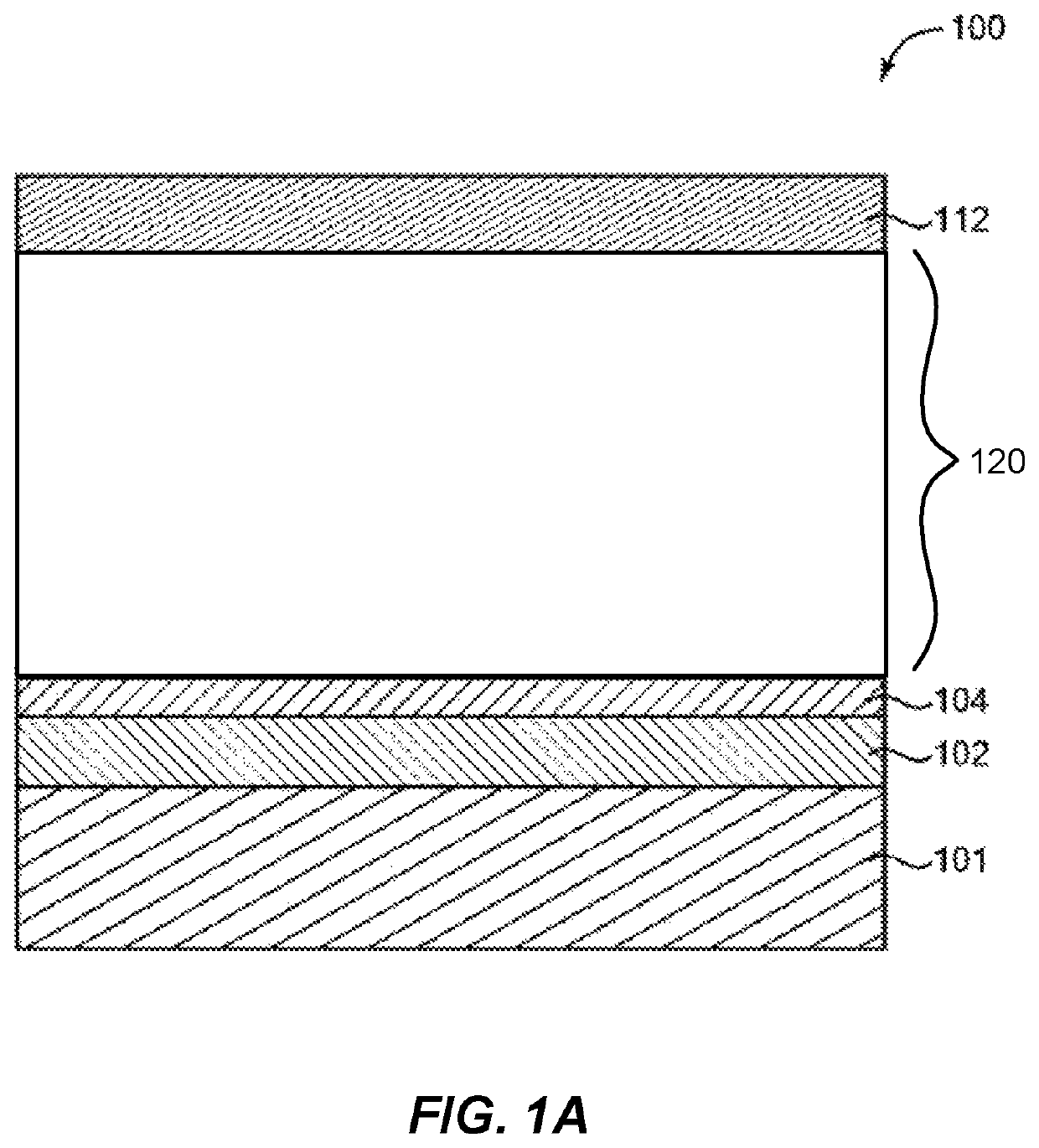
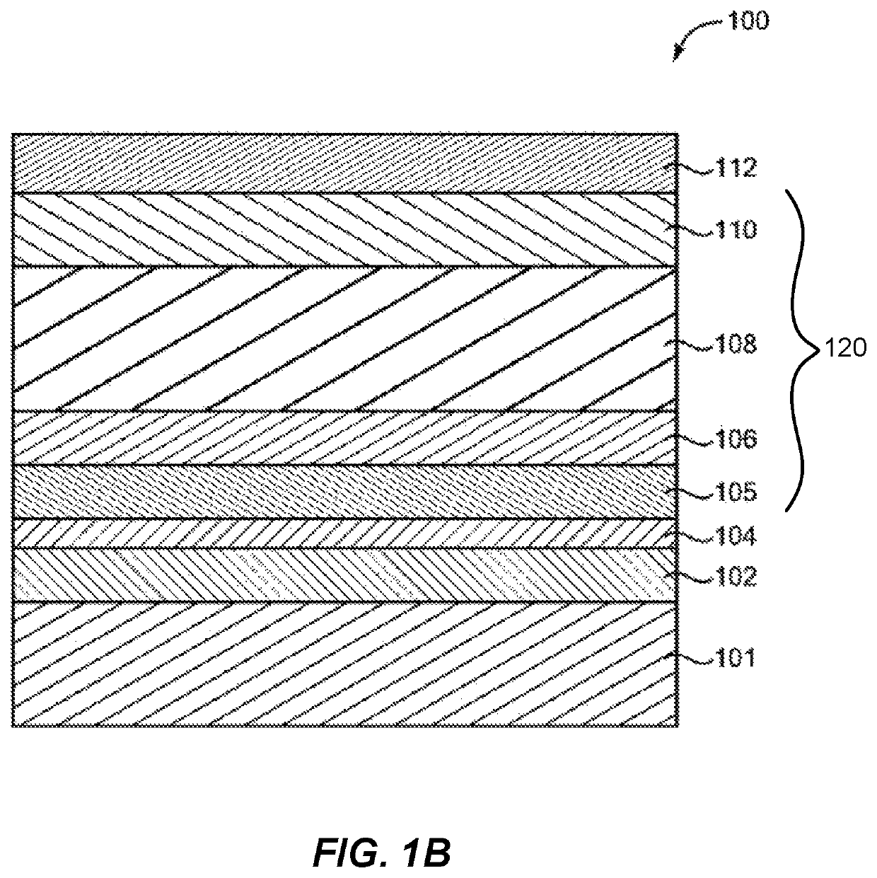
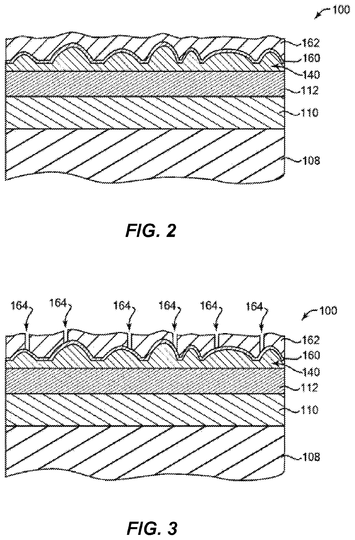
[0030]Various aspects of this disclosure generally relate to optoelectronic devices and processes, and more specifically to optoelectronic semiconductor devices including one or more textured layers and the fabrication processes for forming such optoelectronic devices. Textured layers in this disclosure may refer to, for example, a semiconductor layer having at least one textured surface, where the semiconductor layer is part of an optoelectronic device.
[0031]Herein, a layer can be described as being deposited “on” or “over” one or more other layers. These terms indicate that the layer can be deposited directly on top of the other layer(s), or can indicate that one or more additional layers can be deposited between the layer and the other layer(s) in some implementations. Also, the other layer(s) can be arranged in any order.
[0032]Various implementations and aspects described herein for PV devices relate to light trapping using textured layer(s) for greater device efficiency. The va...
PUM
Property
Measurement
Unit
thick
aaaaa
aaaaa
thickness
aaaaa
aaaaa
thickness
aaaaa
aaaaa
Abstract
An optoelectronic device having a textured layer is described. In an aspect, a method may be used to produce the optoelectronic device, where the method includes epitaxially growing a semiconductor layer of the optoelectronic device on a growth substrate, and exposing the semiconductor layer to an etching process to create at least one textured surface in the semiconductor layer. The textured semiconductor layer can be referred to as a textured layer. The etching process is performed without the use of a template layer, or similar layer, configured as a mask to generate the texturing. The etching process can be done by one or more of a liquid or solution-based chemical etchant, gas etching, laser etching, plasma etching, or ion etching. The method can also include lifting the semiconductor layer of the optoelectronic device from the growth substrate by, for example, the use of an epitaxial lift off (ELO) process.
Description
CROSS-REFERENCE TO RELATED APPLICATIONS[0001]This application is a Continuation-in-Part Application of U.S. patent application Ser. No. 15 / 340,560, filed Nov. 1, 2016, which is a Continuation of U.S. patent application Ser. No. 14 / 452,393, filed Aug. 5, 2014, now U.S. Pat. No. 9,502,594, issued Nov. 22, 2106, which is a Continuation-in-Part Application of U.S. patent application Ser. No. 13 / 354,175, filed Jan. 19, 2012, now U.S. Pat. No. 9,136,422, issued Sep. 15, 2015. The disclosure of each of the priority applications is hereby incorporated in its entirety by reference.BACKGROUND OF THE DISCLOSURE[0002]Implementations of the disclosure generally relate to optoelectronic semiconductor devices, sometimes simply referred to as optoelectronic devices, such as photovoltaic (PV) devices including solar cells, or light emitting diodes (LEDs), and methods for fabricating such devices.[0003]The use of optoelectronic devices, such as PV devices and LEDs, is becoming more widespread as ener...
Claims
Application Information
Patent Timeline
Application Date:The date an application was filed.
Publication Date:The date a patent or application was officially published.
First Publication Date:The earliest publication date of a patent with the same application number.
Issue Date:Publication date of the patent grant document.
PCT Entry Date:The Entry date of PCT National Phase.
Estimated Expiry Date:The statutory expiry date of a patent right according to the Patent Law, and it is the longest term of protection that the patent right can achieve without the termination of the patent right due to other reasons(Term extension factor has been taken into account ).
Invalid Date:Actual expiry date is based on effective date or publication date of legal transaction data of invalid patent.

