Femtosecond laser processing device and method for rapid deep etching of silicon carbide

A kind of femtosecond laser processing and femtosecond laser technology, which is applied in laser welding equipment, metal processing equipment, manufacturing tools, etc., can solve the problems of undercutting, samples that are difficult to etch masks, and needs, etc., and achieve etching processing parameters The setting is fine, avoiding adverse effects, and improving the effect of surface quality

Active Publication Date: 2019-10-29
XI AN JIAOTONG UNIV
View PDF19 Cites 35 Cited by
  • Summary
  • Abstract
  • Description
  • Claims
  • Application Information

AI Technical Summary

Problems solved by technology

Among them, molten salt corrosion requires the use of mixed and molten NaOH / KOH at 480 ° C. This molten salt has the characteristics of high temperature and high corrosion, and has the following disadvantages: ① expensive Pt is required to make the beaker and clamping device for corrosion, ② it is difficult to etch The sample of the mask and the expected structure are obtained, because it is difficult to find a mask material that can withstand high temperature and strong corrosion environment. Even if Pt is used to make the mask, the wet etching is isotropic and will form undercutting
[0005] At present, the femtosecond laser only performs superficial (less than 100 μm) etching processing on materials (such as amorphous silicon, sapphire), and has no effect on the etching quality (depth error of the etching area, surface roughness, and steep sidewalls). degree) to make clear requirements, and currently there is a lack of effective means for fast, high-quality deep etching of silicon carbide using femtosecond lasers
[0006] In addition, the focal plane calibration of laser processing generally adopts three methods: one is to use the laser beam to cut different grooves on the reference workpiece to find the minimum groove width; this method has more cutting times and is relatively complicated
The second is to use the CCD camera to capture the spot of the laser beam irradiated on the surface of the workpiece, and find the minimum value of the spot area; this method requires additional equipment and requires high precision for the graphics processing software
The third is to use a photodiode to measure the light intensity of the laser beam after it is reflected on the surface to be processed, and find the maximum light intensity value; this method also requires additional equipment, and requires high precision for the light intensity processing software

Method used


Image

  • Femtosecond laser processing device and method for rapid deep etching of silicon carbide
  • Femtosecond laser processing device and method for rapid deep etching of silicon carbide
  • Femtosecond laser processing device and method for rapid deep etching of silicon carbide

Examples


example 1

[0134] Example 1: Etching circular blind holes

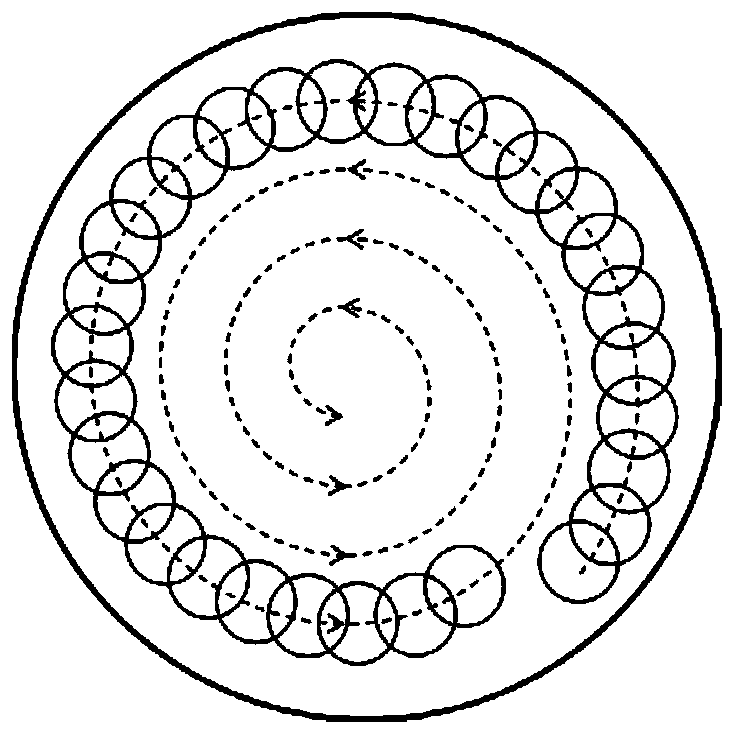
[0135] Etch circular blind holes, design blind hole depth 250μm, diameter 1200μm. High-quality, fast deep etching with femtosecond laser processing equipment. Femtosecond laser processing equipment such as Figure 10 As shown, the aperture of the adjustable aperture 108 is adjusted to 1.4 mm, the focal length of the shaping mirror 109 is 100 mm, the focal length of the plano-convex lens 1010 is 100 mm, and the clamping table 1014 is a vacuum adsorption clamping table. Etching process such as Figure 14 shown.

[0136] (1) According to figure 1 In this method, a femtosecond laser beam is used to ablate two superimposed borosilicate glass sheets for focal plane calibration. The thickness of each borosilicate glass sheet is 350 μm.

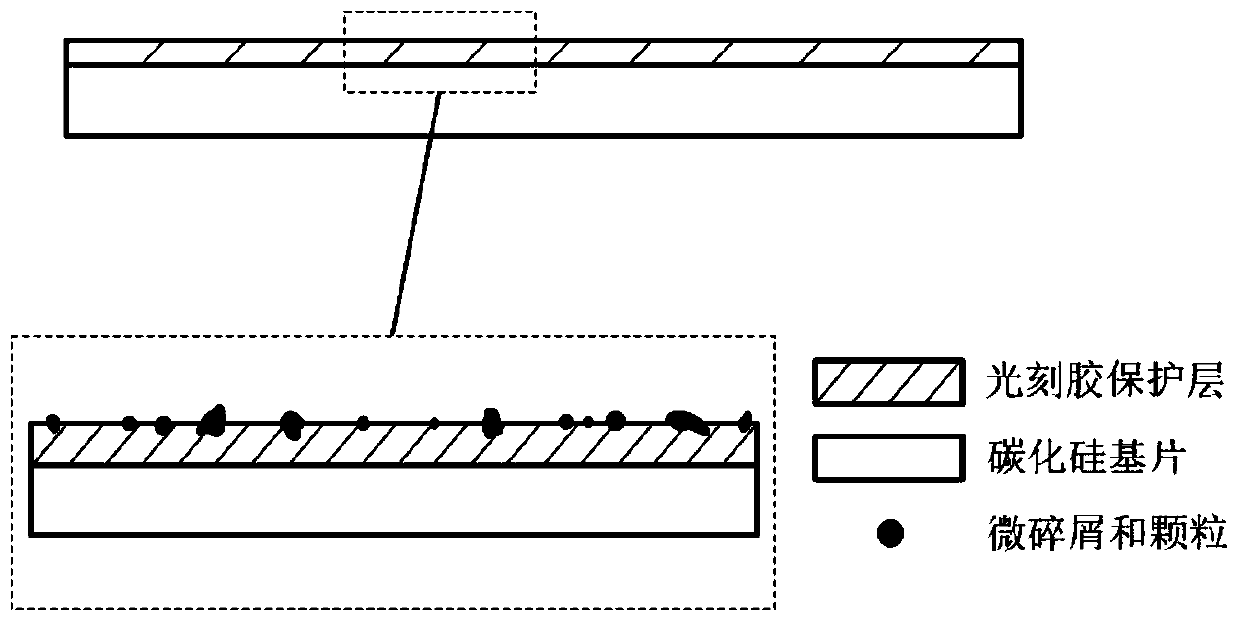
[0137] (2) Select a 4H-SiC substrate with a thickness of 350 μm as the etching object to prepare a photoresist protective layer: wash the 4H-SiC substrate with deionized water for 10 minutes and ...

example 2

[0146] Example 2: Etching square vias

[0147] Etch a square through hole, design the depth of the square hole to be 300 μm, and the side length to be 500 μm. High-quality, fast deep etching with femtosecond laser processing equipment. Femtosecond laser processing equipment such as Figure 10 As shown, the aperture of the adjustable aperture 108 is adjusted to 1.4 mm, the focal length of the shaping mirror 109 is 50 mm, the focal length of the plano-convex lens 1010 is 50 mm, and the clamping table 1014 is a clip-type clamping table. Etching process such as Figure 16 shown.

[0148] (1) According to figure 1 In this method, a femtosecond laser beam is used to ablate two superimposed borosilicate glass sheets for focal plane calibration. The thickness of each borosilicate glass sheet is 300 μm.

[0149] (2) A 6H-SiC substrate with a thickness of 300 μm was selected as an etching object to prepare a photoresist protective layer: the 6H-SiC substrate was cleaned with deion...


PUM

PropertyMeasurementUnit
thicknessaaaaaaaaaa
diameteraaaaaaaaaa
surface roughnessaaaaaaaaaa

Abstract

The invention discloses a femtosecond laser processing device and method for rapid deep etching of silicon carbide. The femtosecond laser processing device mainly comprises a laser source module, a laser motion module, a shaping and focusing module, an auxiliary gas module and a laser etching module. According to the device and method, a focal plane is calibrated, a protection layer is prepared, an etching path is planned, layer-by-layer scanning etching is carried out according to parameter groups, and micro-chips are removed, so that deep etching of silicon carbide is realized. According tothe method, due to the fact that a femtosecond laser is used for processing silicon carbide, factors influencing the etching quality are controlled, namely, the laser energy density, the light spot overlapping rate and the line overlapping rate, and therefore silicon carbide is subjected to rapid and high-quality deep etching in a layer-by-layer scanning manner and a continuous feeding processingmanner according to the planned etching path.

Description

technical field [0001] The invention relates to the field of silicon carbide (silicon carbide) material etching processing, in particular to a femtosecond laser processing method and device for high-quality, fast and deep etching of silicon carbide. Background technique [0002] Silicon carbide (SiC) material is a compound material with unique physical and chemical properties. It not only has superior mechanical properties and physical and chemical stability, but also exhibits superior electrical properties and has a wide band gap (2.3-3.3eV) , high critical electric field strength (0.8~3MV / cm), high saturation drift rate (2×10 7 cm / s) and high thermal conductivity (4.9Wcm -1 K -1 ) characteristics, these characteristics make silicon carbide have important application value in the field of wide bandgap semiconductor high temperature, high power, high frequency and radiation resistant electronic devices. [0003] However, due to the high hardness of the silicon carbide mat...

Claims


Application Information

Patent Timeline
Patent Type & Authority Applications(China)
IPC IPC(8): B23K26/06B23K26/0622B23K26/364B23K26/402B23K26/70
CPCB23K26/0626B23K26/402B23K26/0622B23K26/364B23K26/702
Inventor 赵友赵玉龙王鲁康
Owner XI AN JIAOTONG UNIV
Why Eureka
Try Eureka