Display device
a display device and display technology, applied in the field of display devices, can solve the problems of severe tolerances of optical components during the manufacture and assembly of the device, and the reduction of the resolution of an imag
- Summary
- Abstract
- Description
- Claims
- Application Information
AI Technical Summary
Benefits of technology
Problems solved by technology
Method used
Image

Examples
first exemplary embodiment
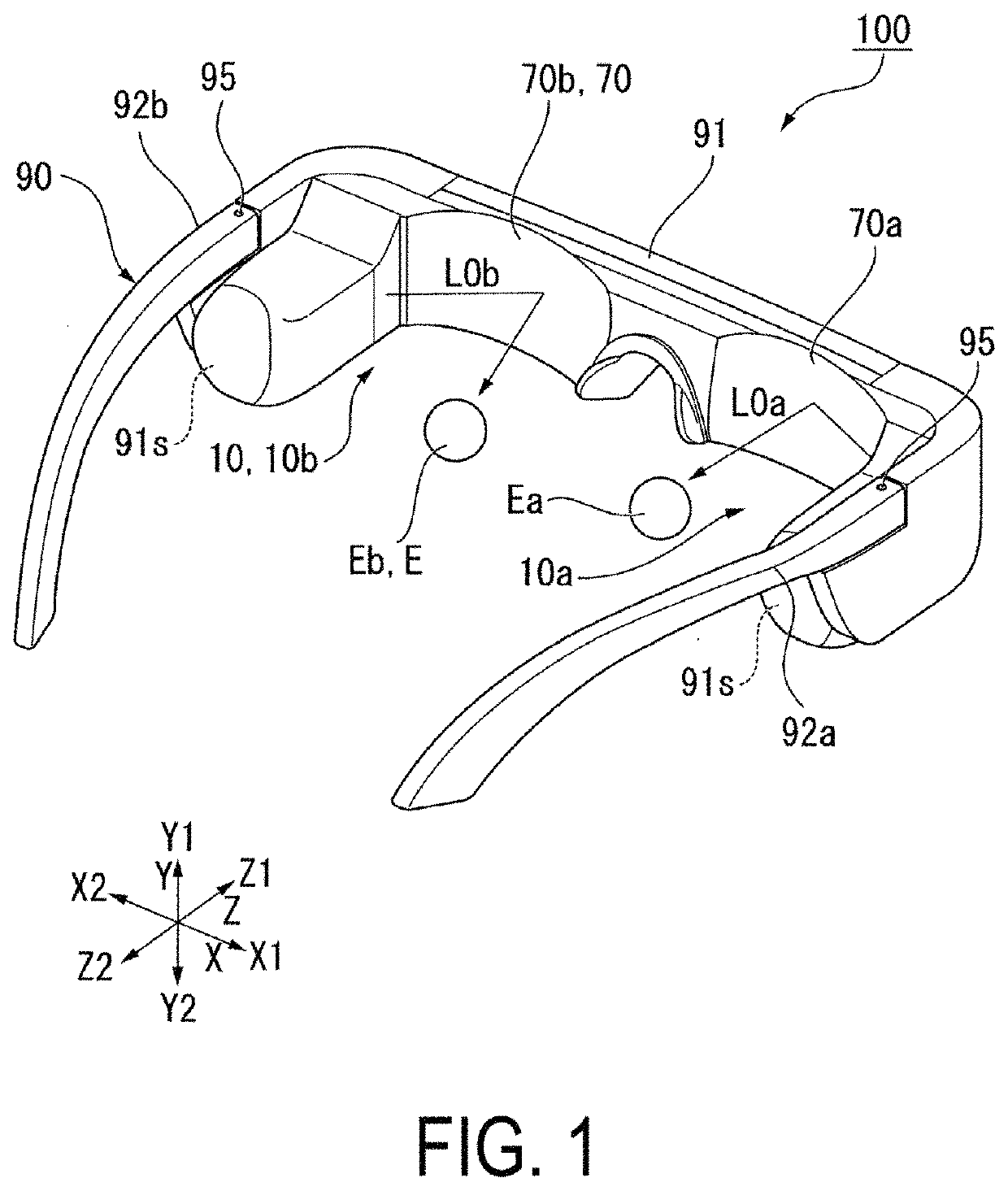
[0033]Exemplary embodiments of the present disclosure will be described below with reference to the accompanying drawings. Note that, in each of the drawings below, to make each of layers and each of members a recognizable size, each of the layers and each of the members are illustrated to be different from an actual scale and an actual angle.
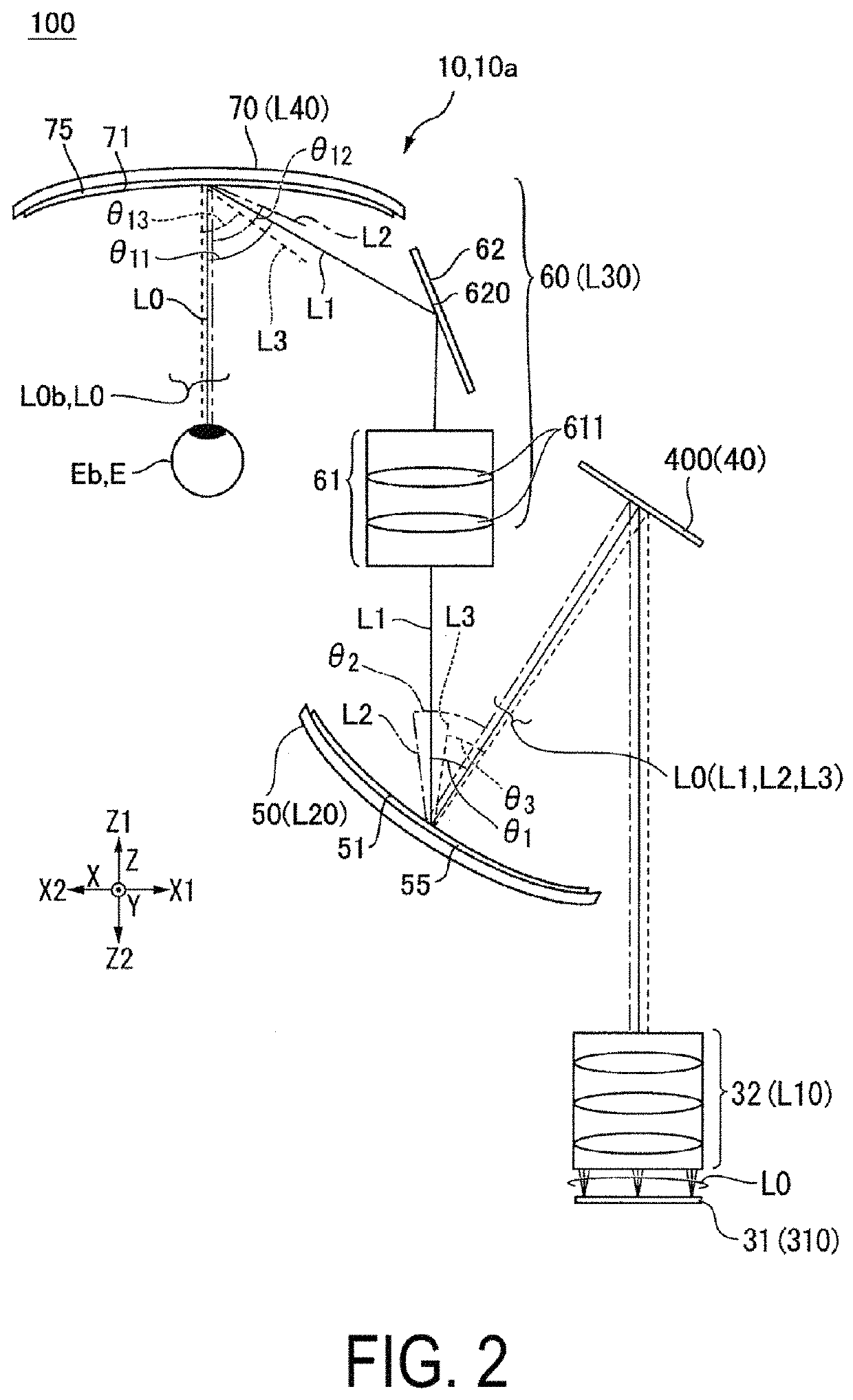
[0034]FIG. 1 is an external view illustrating one aspect of a visual appearance of a display device 100 according to the present exemplary embodiment. FIG. 2 is an explanatory view illustrating one aspect of an optical system 10 of the display device 100 illustrated in FIG. 1. Note that, in FIG. 1 and FIG. 2, a front-back direction relative to an observer wearing the display device is referred to as a direction along a Z axis, an area in front of the observer wearing the display device, which is one side in the front-back direction, is referred to as a front side Z1, and an area in back of the observer wearing the display device, which is the o...
second exemplary embodiment
[0102]Next, a configuration of the optical system according to a second exemplary embodiment will be described.
[0103]The optical system of the present exemplary embodiment has the same power as the optical system 10 of the first exemplary embodiment in the primary diffraction plane, but has a power different from that of the optical system 10 of the first exemplary embodiment in the secondary diffraction plane. In the description below, components common to those of the first exemplary embodiment will be given identical reference numerals and detailed description thereof will be omitted.
[0104]FIG. 10 is a light beam diagram of the secondary diffraction plane of the optical system according to the present exemplary embodiment. Note that the light beam diagram of the secondary diffraction plane of the optical system according to the present exemplary embodiment is common to that in FIG. 7A, and therefore is omitted.
[0105]As illustrated in FIG. 10, in the secondary diffraction plane of...
third exemplary embodiment
[0116]Next, a configuration of the optical system according to a third exemplary embodiment will be described. The optical system of the present exemplary embodiment differs from that of the first exemplary embodiment in the configuration of the imaging light generation device. In the description below, components common to those of the first exemplary embodiment will be given identical reference numerals and detailed description thereof will be omitted.
[0117]FIG. 11 is a light beam diagram of an optical system 10B according to the third exemplary embodiment. Note that FIG. 11 illustrates a configuration of an optical system of the primary diffraction plane. As illustrated in FIG. 11, the optical system 10B of the present exemplary embodiment, similar to the configuration of the first exemplary embodiment, is provided with the first optical portion L10 having a positive power, the second optical portion L20 including the first diffraction element 50 and having a positive power, the ...
PUM
| Property | Measurement | Unit |
|---|---|---|
| wavelength range | aaaaa | aaaaa |
| wavelength range | aaaaa | aaaaa |
| wavelength range | aaaaa | aaaaa |
Abstract
Description
Claims
Application Information