Image processing chip test method

a technology of image processing and test method, applied in the direction of instruments, static indicating devices, etc., can solve the problems of serious problems that can be found, and achieve the effect of accurately and automatically and accurately detected

Active Publication Date: 2021-12-14
REALTEK SEMICON CORP
View PDF2 Cites 0 Cited by
  • Summary
  • Abstract
  • Description
  • Claims
  • Application Information

AI Technical Summary

Benefits of technology

[0004]One objective of the present invention is to provide an image chip test method which can automatically and accurately detect an erroneous operating voltage.
[0005]Another objective of the present invention is to provide an image chip test system which can automatically and accurately detect an erroneous operating voltage.
[0008]In view of above-mentioned embodiments, the image processing chip can be automatically and accurately detected. In such way, the conventional issue that the erroneous operating voltage could not be automatically and accurately detected can be improved.

Problems solved by technology

However, only serious problems can be found by such method.
If the display only has slight problems, the tester may not find the operating voltage is wrong since the image with problems may not obvious or only shows up in a very short time.

Method used


Image

  • Image processing chip test method
  • Image processing chip test method
  • Image processing chip test method

Examples


Embodiment Construction

[0014]Several embodiments are provided in following descriptions to explain the concept of the present invention. Each component in following descriptions can be implemented by hardware (e.g. a device or a circuit) or hardware with software (e.g. a program installed to a processor). Besides, the method in following descriptions can be executed by programs stored in a non-transitory computer readable recording medium such as a hard disk, an optical disc or a memory. Besides, the term “first”, “second”, “third” in following descriptions are only for the purpose of distinguishing different one elements, and do not mean the sequence of the elements. For example, a first device and a second device only mean these devices can have the same structure but are different devices.

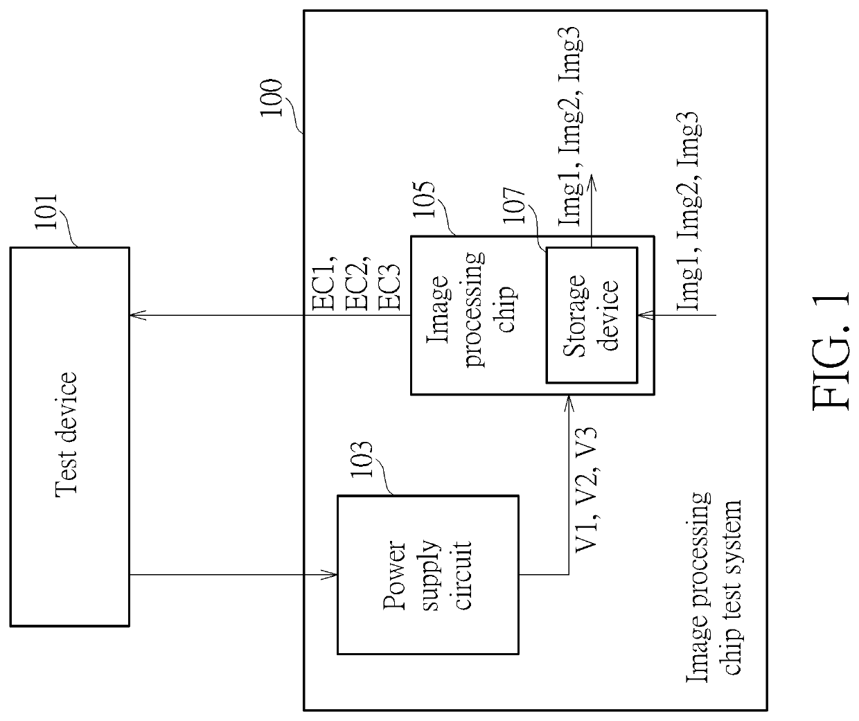
[0015]FIG. 1 is a block diagram illustrating an image processing chip test system using the image processing chip test method according to one embodiment of the present invention. AS shown in FIG. 1, the image process...


PUM


Abstract

An image processing chip test method comprising: controlling a power supply circuit to provide a first operating voltage to an image processing chip comprising a storage device; and when reading written first image data from the storage device, the test device receives a first error detection code corresponding to the first image data and determines whether the first error detection code means an error occurs. If an error occurs, record the first operating voltage as an erroneous operating voltage, and if the error does not occur, provide a second operating voltage to the image processing chip. Also, when the written second image data is read from the storage device, the test device receives a second error detection code corresponding to the second image data and determines whether the second error detection code means an error occurs.

Description

BACKGROUND OF THE INVENTION1. Field of the Invention[0001]The present invention relates to an image processing chip test method, and particularly relates to an image processing chip test method which can automatically test an erroneous operating voltage of an image processing chip.2. Description of the Prior Art[0002]Conventionally, am operating voltage provided to an image processing chip is manually adjusted when a test of the image processing chip is performed. Also, a display connected to the image processing chip is monitored to see if any problem occurs on the display, such as flashing or image string, to determine whether the operating voltage is proper or not.[0003]However, only serious problems can be found by such method. If the display only has slight problems, the tester may not find the operating voltage is wrong since the image with problems may not obvious or only shows up in a very short time.SUMMARY OF THE INVENTION[0004]One objective of the present invention is to ...

Claims


Application Information

Patent Timeline
Patent Type & Authority Patents(United States)
IPC IPC(8): G09G3/00
CPCG09G3/006G09G2330/12G09G2330/028G09G2330/021G09G2310/0259
Inventor HUANG, ZONG-DAYANG, CHING-LAN
Owner REALTEK SEMICON CORP
Why Eureka
Try Eureka