Adjustable via dimension and chamfer angle

a via and angle technology, applied in the field of adjustable via dimensions and chamfer angles, can solve the problems of shorting between adjacent interconnects, chamfering at the top corners of vias, and typically not protecting vias

Active Publication Date: 2022-03-15
INT BUSINESS MASCH CORP
View PDF14 Cites 0 Cited by
  • Summary
  • Abstract
  • Description
  • Claims
  • Application Information

AI Technical Summary

Problems solved by technology

With conventional approaches, however, the vias are typically not protected during the subsequent trench etch step.
As a result, the sidewalls of the via are also etched causing chamfering at the top corners of the vias.
This chamfering can undesirably lead to shorting between adjacent interconnects.

Method used


Image

  • Adjustable via dimension and chamfer angle
  • Adjustable via dimension and chamfer angle
  • Adjustable via dimension and chamfer angle

Examples


Embodiment Construction

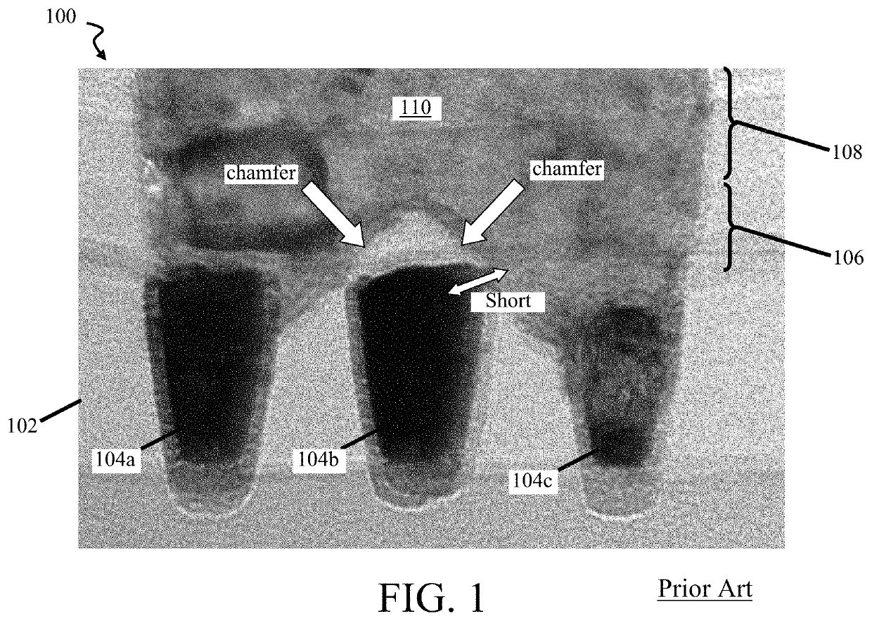
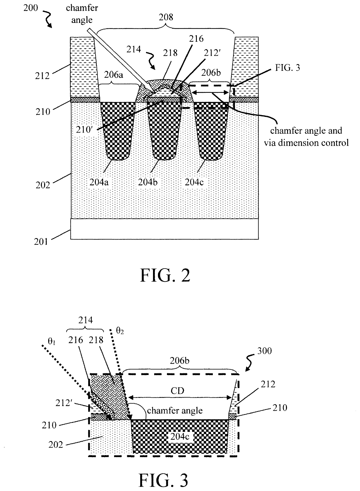
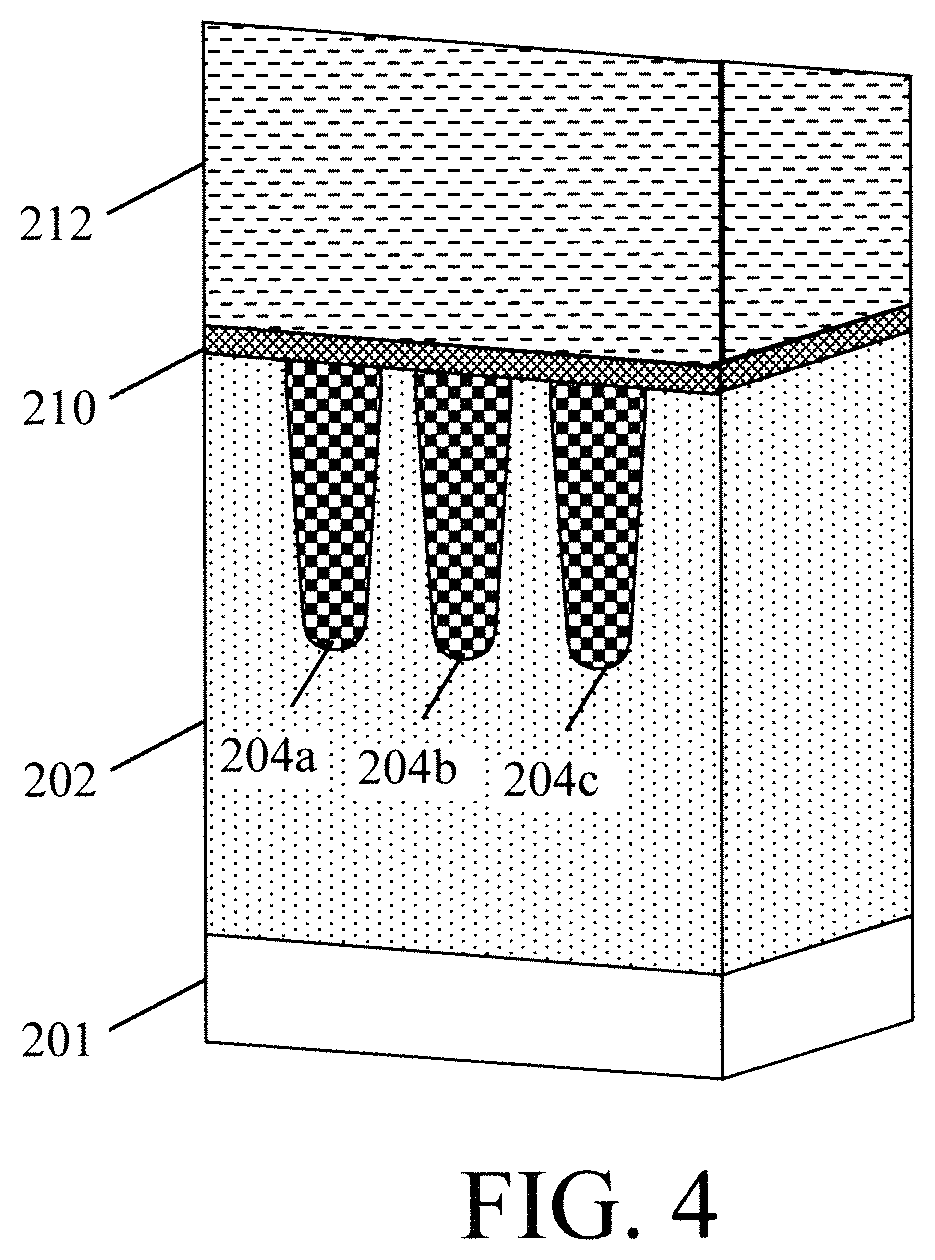
[0019]As provided above, conventional dual damascene processes can introduce chamfering at the tops of the vias. As shown in FIG. 1, this chamfering can undesirably lead to shorting between the interconnect and adjacent structures. Namely, FIG. 1 is an image 100 of a device structure having multiple metal lines, i.e., metal lines 104a, 104b and 104c, embedded in a dielectric 102. In this example, the goal is to contact the two outer metal lines (i.e., metal lines 104a and 104c), but not the center metal line (i.e., metal line 104b). To do so, a dual damascene process is employed whereby vias 106 and a trench 108 are patterned in the dielectric 102 with the vias 106 over the two outer metal lines (i.e., metal lines 104a and 104c) and the trench 108 over the vias 106.

[0020]However, the problem arises that, if un-protected, the sidewalls of the vias 106 are also etched during the trench 108 etch leading to chamfering of the vias 106. See FIG. 1. This chamfering can undesirably expose t...


PUM

PropertyMeasurementUnit
thicknessaaaaaaaaaa
dielectric constantaaaaaaaaaa

Abstract

Chamfer-less via interconnects and techniques for fabrication thereof with a protective dielectric arch are provided. In one aspect, a method of forming an interconnect includes: forming metal lines in a first dielectric; depositing an etch stop liner onto the first dielectric; depositing a second dielectric on the etch stop liner; patterning vias and a trench in the second dielectric, wherein the vias are present over at least one of the metal lines, and wherein the patterning forms patterned portions of the second dielectric / etch stop liner over at least another one of the metal lines; forming a protective dielectric arch over the at least another one of the metal lines; and filling the vias / trench with a metal(s) to form the interconnect which, due to the protective dielectric arch, is in a non-contact position with the at least another one of the metal lines. An interconnect structure is also provided.

Description

FIELD OF THE INVENTION[0001]The present invention relates to via interconnects, and more particularly, to chamfer-less via interconnects and techniques for fabrication thereof employing a controllable via chamfer angle and dimension with a protective dielectric arch.BACKGROUND OF THE INVENTION[0002]In semiconductor fabrication, a dual damascene process can be employed to create metal interconnects. In general, a dual damascene process involves patterning features such as vias and trenches in a dielectric, and then filling the features with metal or metals to form the interconnects. When the vias are patterned before the trenches, this is often referred to as a via-first process.[0003]With conventional approaches, however, the vias are typically not protected during the subsequent trench etch step. As a result, the sidewalls of the via are also etched causing chamfering at the top corners of the vias. This chamfering can undesirably lead to shorting between adjacent interconnects.[00...

Claims


Application Information

Patent Timeline
Patent Type & Authority Patents(United States)
IPC IPC(8): H01L23/522H01L21/768H01L23/528
CPCH01L23/5226H01L21/76807H01L21/76816H01L21/76831H01L21/76877H01L23/5283H01L21/76808H01L2221/1063H01L21/76804
Inventor CLEVENGER, LAWRENCE A.MOTOYAMA, KOICHIMUTHINTI, GANGADHARA RAJAPEETHALA, CORNELIUS BROWNBRIGGS, BENJAMIN D.RIZZOLO, MICHAEL
Owner INT BUSINESS MASCH CORP
Why Eureka
Try Eureka