Touch sensor

Active Publication Date: 2022-10-11
DONGWOO FINE CHEM CO LTD
View PDF21 Cites 0 Cited by
  • Summary
  • Abstract
  • Description
  • Claims
  • Application Information

AI Technical Summary

Benefits of technology

[0029]According to the touch sensor of the present invention, by separating and disposing the transmitter and the receiver touch sensor electrode layers on the opposite surfaces of the substrate, it can be robust against noise from the display unit, and as a result, the recognition sensitivity and recognition rate of the touch sensor can be greatly increased.
[0030]In addition, according to the

Problems solved by technology

However, when the touch sensor is disposed on the upper portion of the display, interference may occur in touch recognition due to noise generated from the display.
In particular, it is very vulnerable to the influence of noise in a structure in which both the transmitter and the receiver touch sensing electrodes are formed

Method used


Image

  • Touch sensor
  • Touch sensor
  • Touch sensor

Examples


Example

[0084]FIGS. 3A to 3E are views showing the first embodiment of a method of manufacturing a display device including a touch sensor according to an embodiment of the present invention.

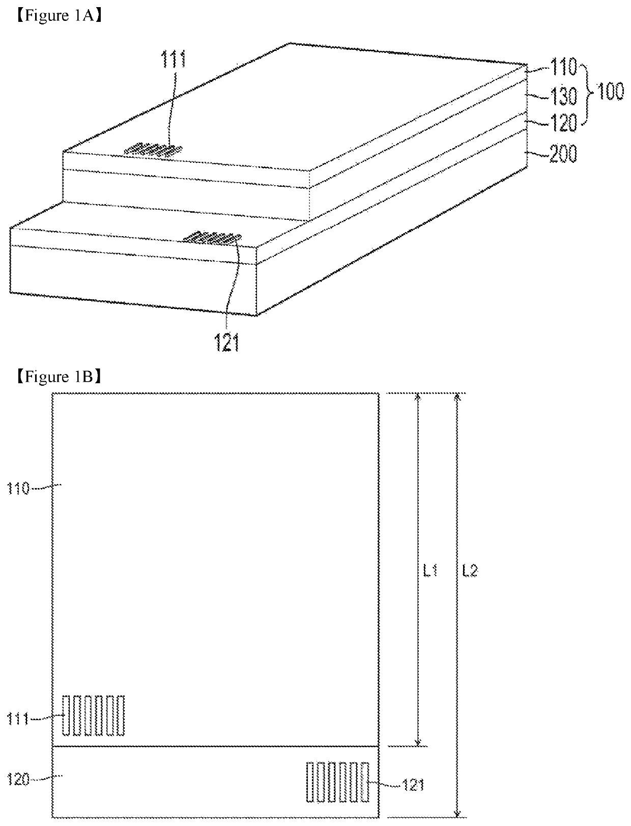
[0085]First, as shown in FIG. 3A, a first touch sensor electrode layer 110 is formed on a first surface of a polarizing plate 130, a second touch sensor electrode layer 120 is formed on a protective film 140, and then the second touch sensor electrode layer 120 is placed on a second surface of the polarizing plate 130.

[0086]At this time, the first and second touch sensor electrode layers 110 and 120 may be formed by a direct transfer method.

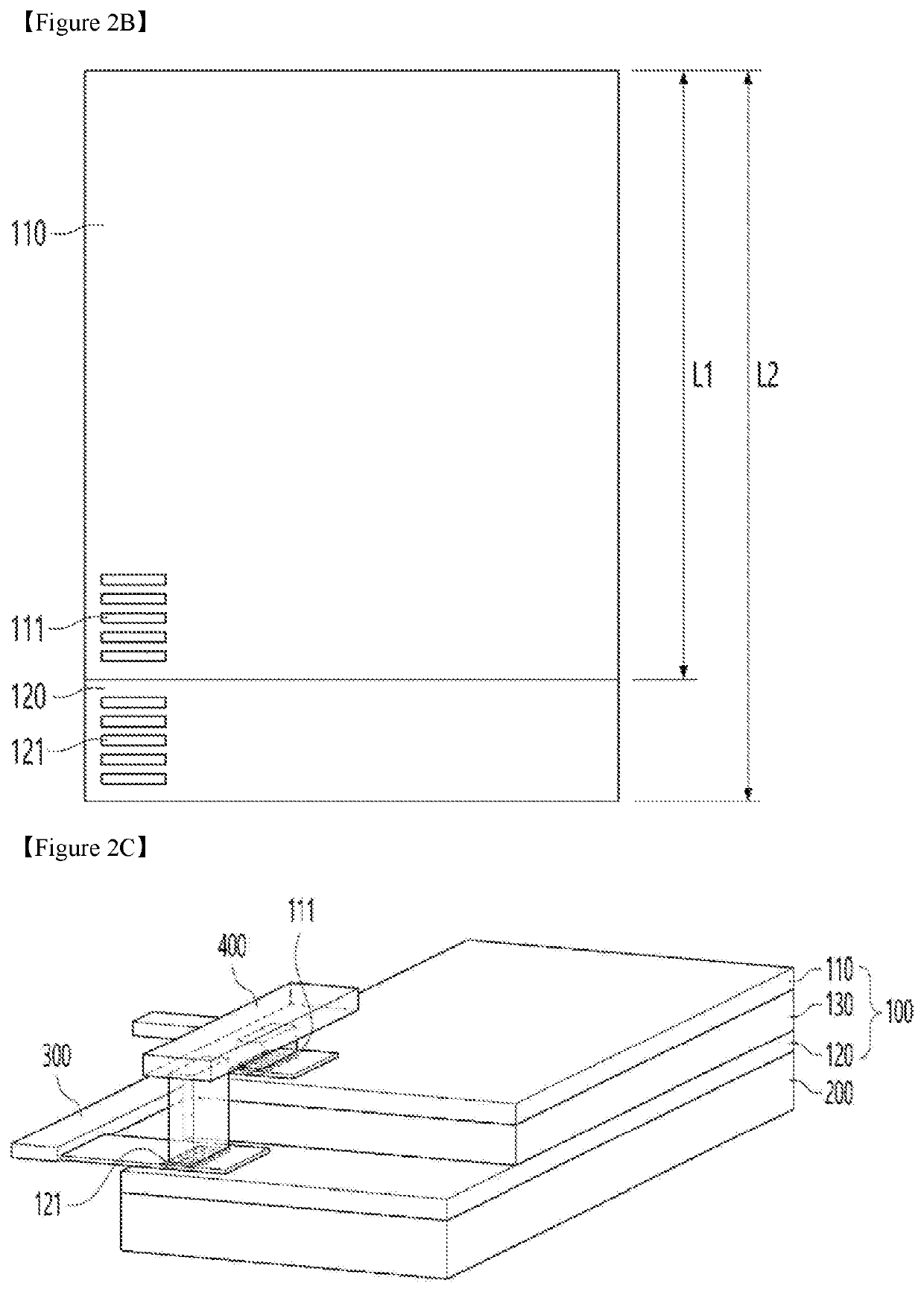
[0087]The first and second touch sensor electrode layers 110 and 120 include first and second pads 111 and 121, respectively.

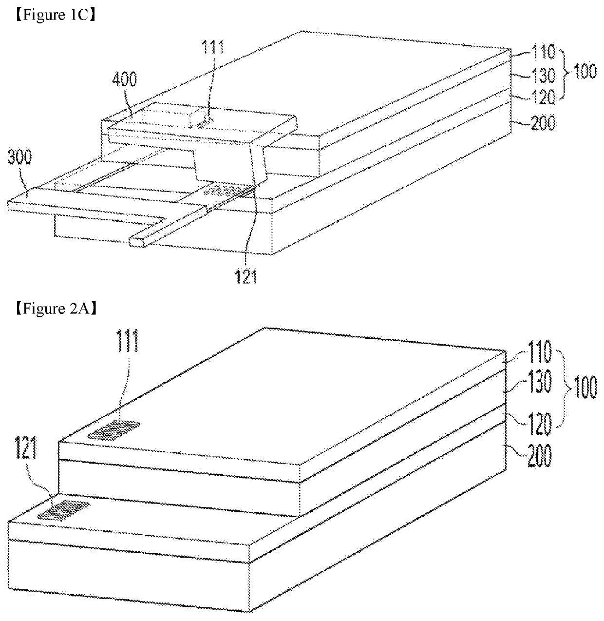
[0088]Next, as shown in FIG. 3B, the protective film 140 is removed, and as shown in FIG. 3C, a display layer 200 is attached.

[0089]And, as shown in FIG. 3D, an FPCB 300 is bonded using a bonding tip 400 having two ends of different lengths cor...

Example

[0091]FIGS. 4A to 4E are views showing the second embodiment of a method of manufacturing a display device including a touch sensor according to an embodiment of the present invention.

[0092]First, as shown in FIG. 4A, a first touch sensor electrode layer 510 is formed on a first surface of a polarizing plate 530, and a second touch sensor electrode layer 520 is formed on a protective film 540 to place the second touch sensor electrode layer 120 on a second surface of the polarizing plate 530.

[0093]At this time, the first and second touch sensor electrode layers 510 and 520 may be formed by a direct transfer method.

[0094]The first and second touch sensor electrode layers 510 and 520 include first and second pads 511 and 521, respectively.

[0095]Next, as shown in FIG. 4B, an FPCB 300 is bonded to the first and second pads 511 and 521 using a bonding tip 400 having two ends of different lengths corresponding to the positions of the first and second pads 511 and 521, respectively, to obt...

Example

[0097]FIGS. 5A to 5E are views showing the third embodiment of a method of manufacturing a display device including a touch sensor according to an embodiment of the present invention.

[0098]As shown in FIG. 5A, a first touch sensor electrode layer 610 is formed on a first surface of a polarizing plate 630, and as shown in FIG. 5B, a second touch sensor electrode layer 620 is formed on a first surface of a display layer 200.

[0099]At this time, the first and the second touch sensor electrode layers 610 and 620 may be formed by a direct transfer method.

[0100]The first and second touch sensor electrode layers 610 and 620 include first and second pads 611 and 621, respectively.

[0101]Next, as shown in FIG. 5C, two laminates shown in FIGS. 5A and 5B, respectively are attached such that the surface on which the second pad 621 of the second touch sensor electrode layer 620 is formed is attached to the second surface of the polarizing plate 630.

[0102]The subsequent process is similar to that i...


PUM


Abstract

A touch sensor includes a substrate and first and second touch sensor electrode layers. The first touch sensor electrode layer is disposed on a first surface of the substrate, and includes a first pad formed on an opposing surface to a surface in contact with the substrate. The second touch sensor electrode layer is disposed on a second surface of the substrate, exposes at least a portion of the surface in contact with the substrate to an outside of the substrate, and includes a second pad formed on the portion exposed to the outside of the surface in contact with the substrate. The first pad and the second pad do not overlap in a stacking direction.

Description

CROSS REFERENCE TO RELATED APPLICATIONS[0001]This is a National Stage of International Application No. PCT / KR2019 / 004595 filed Apr. 16, 2019, claiming priority based on Korean Patent Application No. 10-2018-0044296 filed Apr. 17, 2018, the contents of all of which are incorporated herein by reference in their entirety.TECHNICAL FIELD[0002]The present invention relates to a touch sensor.BACKGROUND ART[0003]Recently, a touch input method in which a user directly touches a screen using a finger to input is widely applied to a display device. The touch input method can provide an intuitive and convenient user interface by allowing a user to touch a specific location on the display screen to input.[0004]In addition, the touch input method can be combined with a display screen without a separate input device such as a keyboard or mouse, which is particularly advantageous for portable electronic devices.[0005]In order to combine the touch input method with the display screen, a touch senso...

Claims


Application Information

Patent Timeline
IPC IPC(8): G06F3/044G02F1/1333H01L51/52G02F1/13363G02F1/1335
CPCG06F3/0443G02F1/13338G02F1/133528G02F1/133634G02F1/133638G06F2203/04103H01L51/5281G02B5/30G06F3/0445H10K59/00H10K59/40G02F1/1333H10K50/86
Inventor TAK, GWANG YONGKIM, JUNHAKIM, JI-YEON
Owner DONGWOO FINE CHEM CO LTD
Why Eureka
Try Eureka