Waveguide bus with balanced optical waveguides and method, system, and software tool for automatic generation of a layout for the waveguide bus
a waveguide and balanced technology, applied in the field of optical waveguides, can solve the problems of time-consuming, inconsistent, prone to errors,
- Summary
- Abstract
- Description
- Claims
- Application Information
AI Technical Summary
Benefits of technology
Problems solved by technology
Method used
Image

Examples
Embodiment Construction
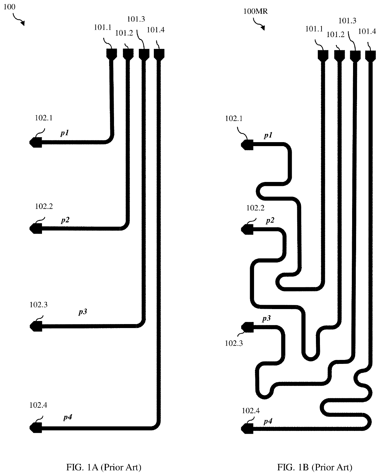
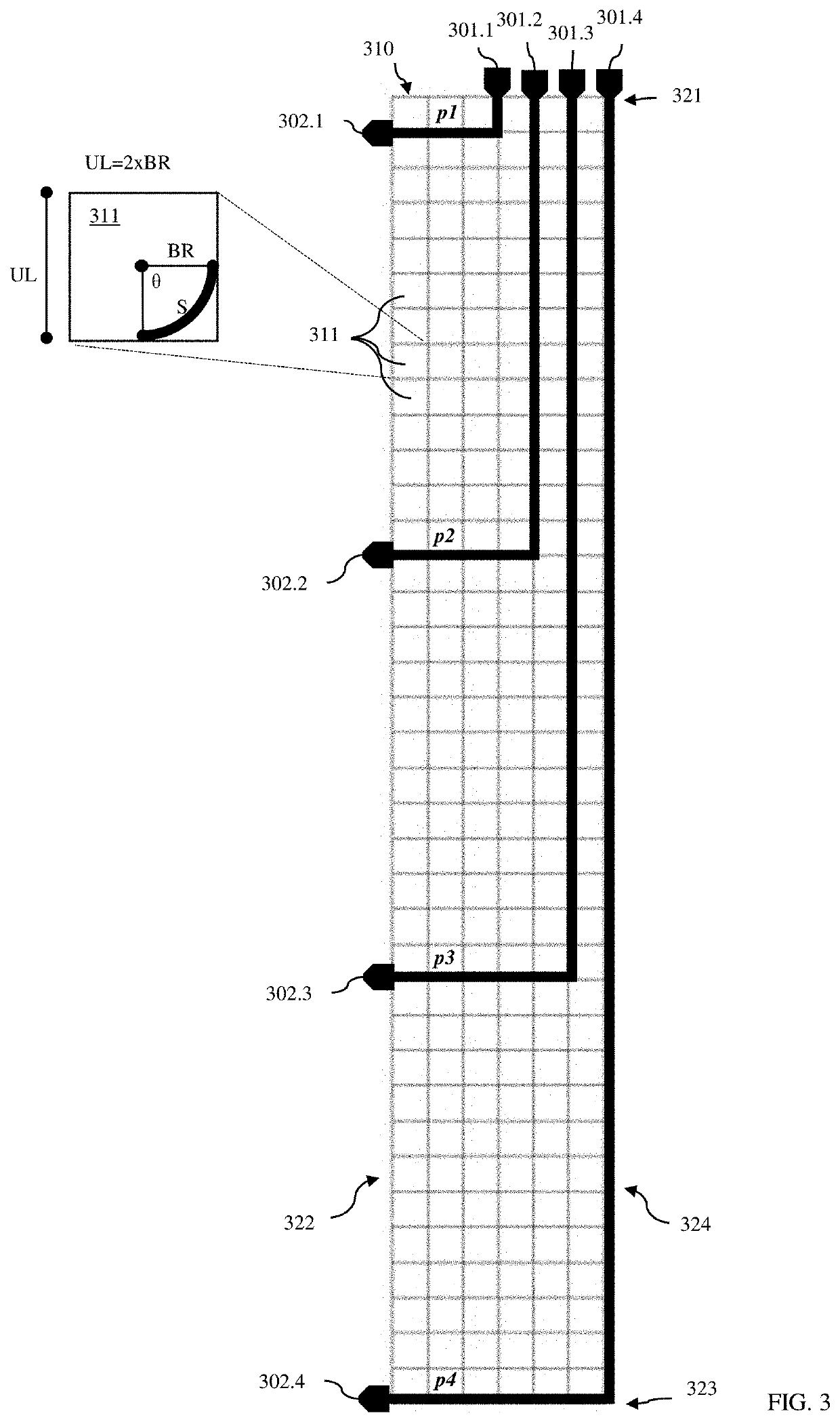
[0023]As mentioned above, a silicon photonic integrated chip (PIC) may include an optical waveguide (WG) bus (i.e., a set of optical WGs). Each of the WGs in the WG bus transmit an optical signal between a pair of input / output nodes. During PIC design, the paths for the optical WGs are automatically laid out (e.g., by a WG layout generation tool) based on design rules that are directed to, for example, critical dimensions, minimizing area consumption, etc. Typically, each path in the resulting automatically generated layout will have the shortest length and fewest number of bends possible between its corresponding input / output nodes. However, some PIC designs require the WGs in a WG bus to be balanced. For purpose of this disclosure, “balanced WGs” refers to WGs that subject optical signals passing therethrough to essentially the same transmission loss and phase shifting. Those skilled in the art will recognize that transmission loss and phase shifting of an optical signal passing t...
PUM
 Abstract
Description
Claims
Application Information